Very nice and would buy one for my business, but they are just TOO expensive! Reduce the price significantly and you would dominate the pcb cnc market. With low cost pcbs on a couple of days turnaround, I can have thousands of prototypes made for less than this ... and no, having it done in an hour or two is not important. My customers dont see a finished product for months, so time is not the critical element ... but COST is!
@Esteban Rodríquez That's right, Esteban, nobody "loves" to solder, they lie if they say they do. I finally learned to live with it. For me, painting the joint with liquid flux first made my life a whole lot easier. I also paint the soldering iron tip with flux before I turn it on.
@Ron Garza not sure if you’re joking or not, but there are certainly people that enjoy soldering...I know because I’m one of them. And no I’m not lying haha
Why? Soldering a board like this is quite easy, even for a beginner. There's lots of great tutorials on how to solder a board like this here on UA-cam.
Have you ever actually hand-soldered a chip with 0.1mm spacing between pads? First-off it is not easy, second - it is almost impossible to do with simple home soldering irons. Third - this board doesn't have solder mask Fourth - this board has very small spacing between traces. Combine that with third - and you get a lot of unwanted bridges between traces - which you will have to clean off - welcome to hell. Even if you will solder every single trace and every single pad and clean all the bridges- you still have to pray that you do not have any bridges underneath the chips. Because if you do - you will know that only once the board starts and doesn't work for unknown reason. Everything looks nice on youtube video, but try it out yourself to see.
@@marc_frank and when and where did he ever told that he did not ever create anything like hell or is going to create or allow it to be created? Don't be too full of yourself and put words in the mouth of the God that he never spoke. There is hell on earth, and there is hell besides earth.
You guys should work on ink-jetting the copper layer onto fiberglass instead of trying to CNC material off the board, CNC has been done thousands of times by others and has yet to really work. If you could work out the chemistry of depositing metal you’d have a winner that could be done with a $25 ink jet print head and have 100 times the resolution of CNC.
Just an addition to your idea , just like through hole plating if you could come up with a method which inkjet prints something which could later be copper plated .......
From my own experience i know how hard it is, to build a machine capable of doing this. You guys did absolutely fantastic. The leveling and the balance of the tools is impressive.
The main problem - non flat surface of board, bended material. Conical mill will produce different cut diameter on different parts of surface. Probably maximum width x height - 6 x 9 cm.
KV, I stick my PCB down to a sacrificial base that screw down to the machine bed. I use very thin double sided tape from Amazon. This keeps the whole copper board flat and then the electrical probing performs a contour map of the surface and the isolation routing is spot on. Using a this flat bladed screw driver and gradual bending force will prise the board from the base, Acetone will clean up both the back side of the PCB and the base as well.
This would be a great machine for RF engineers - they could tinker with circuit layouts without the wait for regular PCB turnaround times - most of their stuff is 2-sided at the most!
@KOMODOR I have a 3020 and while I have made good PCBs from it, it's no where near the quality of this thing. For example, the runout of the spindle is 0.1mm so good luck getting those same traces as in the video
Very slow production rate, etching makes finer trace and space, and you often cannot leave so much unconnected conductive material. Cool capability though.
I mean it's about rapid prototyping man. We have one in our lab (not this companies) its made by LPKF they are exceptionally capable. Even have plate thru hole capability, it's not done the way shown here tho. Sometimes sending out for PCB fabrication also means exposing what you're working on...
It is beautiful... From practical point of view. It would ve amazing if you can show, how the components are soldered onto it. I mean the melted tin just flow everywhere as there is no protective layer on that board. Even if using paste and heat gun
Peter, after the isolation and drilling process you clean the board and apply solder resist. One dry you use the an engraving bit and this mills through the solder resist to expose the component pads only. The rest of the board is protected by the resist. Hopefully this makes sense.
1. Не верные обороты резца. 2. Не верна скорость подачи. 3. Такой ровный текстолит не найти в моей стране. 4. Выбирать остальную медь запаришься, травление лучше (по скрости). 5. Ну и скорость соответственно, одну плату повесишься ждать. Никто не спорит за качество и красоту, но смысла в этом мало, не целесобразно. Говорю как чпушник и радиоинженер.
@@bato1903 на таких оборотах, с такой нагрузкой, перегреет и сломает кончик - там не 24 000об/мин)) угловая скорость реза на диаметре 0,1 мм, деббил!))- радиогубитель)) ты чпу только на картинке видел, по всей видимости?) Понаберут клоунов по объявлению..)
Arrgh! Cutting out the board BEFORE milling the reverse side!?!?! What a bone-headed move! Mill both sides, then cut out the board-outlines as a final step.
Where did you start doing this?Is it on a cad or cnc either way I did both in highschool but it's been a while & then did you transferred it to this software to car out the blueprint on the copper pcb?
Better hope your material is perfectly flat, which of course it won’t be, unless your paying an absolute fortune for extremely high quality PCB blanks. Seems only very expensive laser machines actually work reliably without hours of hassle at this point. In the end, it’s still going to be cheaper, and far far higher quality just getting a board house to use their millions of dollars worth of equipment to build them for you. Very neat concept that unfortunately still needs huge amounts of further design work to be practical, such as having sensors for dealing with less than perfect material stock and bit wear, professional machines use cameras for visual inspection and probing to overcome this. Rivets to join layers have been around for decades and sorta work for repairs if you only have one or two, on a board with lots of them you’ll have to solder them or you’ll have intermittent connection problems. So you might as well just run a jumper wire and solder that.
за огромные бабки - предлагается абсолютно ненужный аппарат.. но подано красиво :))) Хотя конечно же за такие деньги можно два вагона плат заказать в китае...
@@TheMirclub _Дешевле заказать качествннные платы, уже с распайкой смд_ Вы видимо невнимательно прочли моё сообщение.. там же написано ровно тоже самое..: prnt.sc/lsxfyn
1 reason an 1 reason only. In house testing without the delay of shipping. If a prototype exits its design phase you can get a working prototype by the end of the day
@@jakeengland1430 you can etch circuitboards at home though? like, all you need is a run of the mill printer, a clothes iron, some acetone, ferric chloride ane a solder mask. You can have a working prototype in less than 20 minutes, assuming you don't have specialised equipment.
@@paweljasiek i from personal experience will never touch acetone again it such a pain to work with and dangerous too its also not as repeatable you can also get much higher resolution on mills yeah for hobbyists go down your route cause its cheaper and easier bt for professionals mills are the way to go.
@@jakeengland1430 You can keep the traces a little thicker in the proto and then thin them down later according to the fab house's capability. I'm assuming these are logic level signals and not power. Regardless, if you really are on the clock, etching is way faster. This is more of a luxury to be honest.
Well a few reasons when compared to a small “Hack” photolithography set up. 1) with a standard at home inkjet printer you will not get down to 100 micron trace widths and spacing. The mask an at home printer does simply cannot produce a fine features like that. When you get that small you eventually start seeing the individual droplets of the print head and the density of the droplets is not high enough. You will etch those lines off. 2) depending on the project RF or Signal lines, the precision of the line widths are very important and you will not be able to do that accurately at home with a hack set up. Over etching is a huge huge problem when the features become small. 50 micron (which is a a very small amount of over etching. Would have to be a 1/4 oz copper) could be a huge percentage of your trace widths. 3) DIY or small operations chemical waste and chemical training is a huge aspect. For professional businesses that are small scale, chemical training and waste are very costly. You’re working with harsh chemicals that need to be disposed off properly. You should also really be utilizing a fume hood. 4) the mill also can drill VIAs and cut out the board to desired shape in one step. You will have to manually do that with photolithography which will never look as good. While a hack photolithography set up is nice and cheap, eventually it will all come to be the same price. Remember etchant doesn’t last forever and has to be replaced, solvents to clean the board need to be bought, other tools are needed for VIAs, and ink for the printer. Also time is money, this will be faster then etching at the hobbiest level. I don’t think you’d be making boards large enough where this would be to slow for that. As a hobbiest I understand this would be a luxury but would be really amazing to have it! This thing looked like a beast!
0.1mm traces? 0.13 - 0.15mm... The contact pitch of TQFP100 is 0.5mm IC!? Contact pad width 0.3mm. and Lead width 0.22mm. Is the distance between the PCB line of the IC about 0.1 mm?
Hi John, it is not too noisy, you can work in a room at the same time. The PCB probe of the copper clad board takes up to 40 minutes and then you can load the nc code to start milling. It gets noisy once you start to mill the board edges. During the isolation routing I like to keep an eye on things every 10 minutes to add a few drops of mineral oil to the copper surface as this greatly improves the cut and final finish.
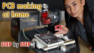
To answer some of the questions below. Sonia have had this machine for over a year now. It is an amazing price of kit and extremely well made. Isolation milling can take e quite some time and as does the probing of the PCB surface prior to milling. This machine can mill a small PCB in about 3 hours if you include the probe and mill operation. Also make sure that you have the correct isolation routing bits for the job. Also weave a small syringe of mineral oil to cot the PCB surface with prior to milling, it makes a big difference to the quality of the cut. With respect to milling the outside profile of the PCB, if the PCB is square or rectangular then far better to use a PCB Guillotine to cut the board. So for a slightly higher volume of birds, day 10 or more, I use this machine to drill all the holes in Microtrak pre-sensitised PCB board and then expose and etch in the usual way. This machine is very precise and accurate however use as intended for very small prototype runs and either use conventional etching or JLCPCB in China for more than say 20 boards. This is an outstanding machine for its intended purpose. I am about to test this out to do some M2 thread milling in aluminium and sure it will be fine.
Музыка оскомину набила! Северный проект под неё пургу гонит)) Честно говоря здесь она более уместна)), но можно и без неё, удовольствия от этого меньше не станет!


It's probably been said, but from an Engineering perspective, this is better than porn
Indeed
Porn damages your brain cells, scientifically proved
@@Enes-wj5xq AND?
@@Enes-wj5xq ok, what about sexual art that's been a part of human culture since post cave-man times? Wooden woman sculptures & that & beyond
@@Enes-wj5xq LOL breathing damages your brain cells too. This one is also scientifically proven
The song goes oioioioioioioioiOioiioioi
Foreigners are amazing, they develop so many machines
I have never seen any such machines get manufactured in my country 😭
Where are you from?
сколько раз уже пересматриваю. Это изумительно!!!!
Так а что это за деталь?
После такокой фрезировки, молток смотрится несколько вульгарно
How amazing it is mann
Seeing the tooth brush fucked me up
Very nice and would buy one for my business, but they are just TOO expensive! Reduce the price significantly and you would dominate the pcb cnc market. With low cost pcbs on a couple of days turnaround, I can have thousands of prototypes made for less than this ... and no, having it done in an hour or two is not important. My customers dont see a finished product for months, so time is not the critical element ... but COST is!
Depois dessa micro estrutura toda pra fazer a placa o cara finalizar com martelada é foda.
Admirando a precisão , e acontece isso '-'
Agora isso vai servir pra que exatamente?
Better than porn
Hehehe lol!! XD
Its mythpaths intro if anu of you guys recognize
"Yo
Yo, yo
Yoyoyoyoyoyoyoyo
Yooyoyoyoyoyoyoyoyoyoyoyoyo
Bing bing bing
YOYOYOYOYOYOYOYOYOYOYOYOYOYOYOYOYOYOYOYO''
Bow dow bow bow
boy yoy oy
Bow
Bow bow
bowbowbow
bowbowbowbow
bowbowbowbowbow
bowbowbowbowbowbow
bowbowbowbowbowbowbow
Pppp
DELAY LAMA LOL
2021 Mat, Poland here: Ojojojojjjj , bzyyyy 🎹🇵🇱
Where the hell do you get such a huge toothbrush?!
It bel8bged to Gulliver
From any regular department store
Title literally: 0.1 mm traces
🤣🤣🤣
everything is fun until you start soldering
What do you mean?
@Esteban Rodríquez That's right, Esteban, nobody "loves" to solder, they lie if they say they do. I finally learned to live with it. For me, painting the joint with liquid flux first made my life a whole lot easier. I also paint the soldering iron tip with flux before I turn it on.
@Ron Garza not sure if you’re joking or not, but there are certainly people that enjoy soldering...I know because I’m one of them. And no I’m not lying haha
@@rongarza9488I love solder...
He will do soldering after coating and go engraving on soldering spots. So, it's extremely easy and still fun.
I watched the entire thing without knowing what the hell is this.
Me too
Me too
Some kind of USB device, like thumb drive or dongle.
Where do i buy that giant toothbrush from?
😂😂😂
Google: Here are some results for "big toothbrushs" *shows a slightly larger toothbrush*
Bing:
Music: oyoyoyoyoyoyoyoyo...
Nobody:
The music: *yoyoyoyoyoyoyoyoy*
ahahahahah
I like how there was a random "here's a match for scale" appearance and I was thinking, whata giant match, lok
Yoyo yoyoyoyoyo yoyo yoyo
Если этот фрезер попутно играет эту музыку - не важно, сколько он стоит.
This is very satisfying
Doioioioioioi
Yoyoyoi
Yo yoyoyoyoi
Ouiouioui
I can’t with the eltectro-reggae music 😂
Magic, it's magic, I can't take my eyes off the screen.
They put down the match for scale but all my brain see is a big ass match
It'd be good to occasionally see it a bit more zoomed out so we can see the whole machine 👍
Oioioioioioooo 🎶
this is the best pcb cnc milling machines I ever see, yet the price is not quite meet the student/hobbyist budget :D
And now... if you will try to solder a chip to this board, you will get to know the seventh level of hell :P
Why? Soldering a board like this is quite easy, even for a beginner. There's lots of great tutorials on how to solder a board like this here on UA-cam.
Have you ever actually hand-soldered a chip with 0.1mm spacing between pads?
First-off it is not easy, second - it is almost impossible to do with simple home soldering irons.
Third - this board doesn't have solder mask
Fourth - this board has very small spacing between traces.
Combine that with third - and you get a lot of unwanted bridges between traces - which you will have to clean off - welcome to hell.
Even if you will solder every single trace and every single pad and clean all the bridges- you still have to pray that you do not have any bridges underneath the chips. Because if you do - you will know that only once the board starts and doesn't work for unknown reason.
Everything looks nice on youtube video, but try it out yourself to see.
Whatever, I have soldered more than enough chips by myself, believe in what you want.
@@marc_frank don't tell the god what he can and cannot do :P
@@marc_frank and when and where did he ever told that he did not ever create anything like hell or is going to create or allow it to be created?
Don't be too full of yourself and put words in the mouth of the God that he never spoke. There is hell on earth, and there is hell besides earth.
You guys should work on ink-jetting the copper layer onto fiberglass instead of trying to CNC material off the board, CNC has been done thousands of times by others and has yet to really work. If you could work out the chemistry of depositing metal you’d have a winner that could be done with a $25 ink jet print head and have 100 times the resolution of CNC.
Just an addition to your idea , just like through hole plating if you could come up with a method which inkjet prints something which could later be copper plated .......
The music was so annoying
I like it! I need Track ID!
Still is
Oyoyoyoyoyoyo
The music makes me very uncomfortable hahaha. But i like how clean the traces ar.
Im lazy but someone needs to post this on reddit in the /oddlysatisfying category!
8:30 oioioioioioi,yoy yoy yoy yoy yoy yoy
Oiooioiooiooi
Video: excellent. Music: unnecessary.
You can low it down and that's all.
YT: Psst hey
Me: Yeah
YT: you still up?
Me: Yeah ( 4:15 am )
YT: Wanna see something satisfying?
Me: sure
Plot twist: it's actually a big toothbrush and measuring ruler
Music is cool, until:
"Yoyo... Yoyoyo... Yoyoyoyoyoyoyoyoyo"
🤣😂🤣😂
From my own experience i know how hard it is, to build a machine capable of doing this. You guys did absolutely fantastic. The leveling and the balance of the tools is impressive.
Тут интересен сам процесс изготовления плат, а не заказ заводских плат. Автор красава, поддерживаю твоё хобби.👍🏻
A lot of questions and no answers.
Imagine drawing some fractals in tiny pieces of metal like this, it would make nice souvenirs
It's giving me eyegasm
Me: in class
UA-cam : RECOMMENDS THIS RANDOM video
The main problem - non flat surface of board, bended material. Conical mill will produce different cut diameter on different parts of surface. Probably maximum width x height - 6 x 9 cm.
KV Popenko you need to make height map. Look up candle.
KV, I stick my PCB down to a sacrificial base that screw down to the machine bed. I use very thin double sided tape from Amazon. This keeps the whole copper board flat and then the electrical probing performs a contour map of the surface and the isolation routing is spot on. Using a this flat bladed screw driver and gradual bending force will prise the board from the base, Acetone will clean up both the back side of the PCB and the base as well.
This was satisfying but it would’ve been better without the music
Just turn the volume off
Reggie Vdz I did but I would rather hear the work being performed
This would be a great machine for RF engineers - they could tinker with circuit layouts without the wait for regular PCB turnaround times - most of their stuff is 2-sided at the most!
I have to say this is one awesome machine, but as a hobbyist the $3,300 price tag is out of my reach. I Cant wait till it gets more affordable.
@KOMODOR I have a 3020 and while I have made good PCBs from it, it's no where near the quality of this thing. For example, the runout of the spindle is 0.1mm so good luck getting those same traces as in the video
Music name is fiction by Amy Reynolds. Your welcome!
oioioioioioioio
Yoyyoyoyoyyoy yoy yoy yoy yoy.
How do we know that is not a giant stick and a giant tooth brush?
Well, i don't know what this is, but it was very satisfying to watch.
Its your hardware robot XD
I think, this was a board of pendrive
The music is just yoyoyoyoyoyoyo
ไฟพุ่ง กับพิมพ์เขียวเส้น มันเรียนรู้ไม่เหมือนกัน แต่ได้เหมือนกัน เหมือน เคเอฟซี กับ ตู้ทอดไก่ คนละสูตร เครื่องเทศ เซิ่น เอามาลองทำเอง อร่อยมาก หอม จมูก เหมือนกิน เลย กับกินเข้าๆไป กินเหมือนกันเลย เหมือนที่ว่า ใช้ทองแดง กับน้ำเจล พริบเดียว 🤣🌙☀️
i watched this video for music
Outclassed background music....😍😍
Very slow production rate, etching makes finer trace and space, and you often cannot leave so much unconnected conductive material. Cool capability though.
I mean it's about rapid prototyping man. We have one in our lab (not this companies) its made by LPKF they are exceptionally capable. Even have plate thru hole capability, it's not done the way shown here tho. Sometimes sending out for PCB fabrication also means exposing what you're working on...
Hurry up and make me a GPU already
yoyo's proyect
It is beautiful...
From practical point of view. It would ve amazing if you can show, how the components are soldered onto it. I mean the melted tin just flow everywhere as there is no protective layer on that board. Even if using paste and heat gun
Peter, after the isolation and drilling process you clean the board and apply solder resist. One dry you use the an engraving bit and this mills through the solder resist to expose the component pads only. The rest of the board is protected by the resist. Hopefully this makes sense.
cool music (oi oi oi), but reminds me of brushing my teeth 😁
08:32 oooo ooeeee ooooeee oooee
Music ruined it
1. Не верные обороты резца.
2. Не верна скорость подачи.
3. Такой ровный текстолит не найти в моей стране.
4. Выбирать остальную медь запаришься, травление лучше (по скрости).
5. Ну и скорость соответственно, одну плату повесишься ждать.
Никто не спорит за качество и красоту, но смысла в этом мало, не целесобразно. Говорю как чпушник и радиоинженер.
Какую рекомендуете скорость и подачу ?
@@IhorKochet подачу медленее, скорость быстрее. Ибо если пылесос тупнет, пылью порвет все дорожки.
@@bato1903 на таких оборотах, с такой нагрузкой, перегреет и сломает кончик - там не 24 000об/мин)) угловая скорость реза на диаметре 0,1 мм, деббил!))- радиогубитель)) ты чпу только на картинке видел, по всей видимости?) Понаберут клоунов по объявлению..)
Я уже давно об этом написал. Что это бесполезный кусок дерьма для изготовления плат. Но находятся особо тугие люди которые с этим спорят.
@@imiafamily Так ты сам признался что ты клоун. Обороты выбираются из состава резца и материала. То что идет по стали, вязнет на люме. Клоуна кусок.
BGM Seems like we are signaling an alien
Specially the Yo oooo eee part
Arrgh!
Cutting out the board BEFORE milling the reverse side!?!?!
What a bone-headed move!
Mill both sides, then cut out the board-outlines as a final step.
This video is so so satisfying
ТОЖЕ ИЩЕШЬ РУССКИЕ КОММЕНТАРИИ?)))))
Зато они гвоздём паять не умеют
Нет, я пишу их)
No, I'm not.
"Nano machines, Son!"
This is satisfying to watch.
I didn't realize how small it was
Until I saw the matchstick
Where did you start doing this?Is it on a cad or cnc either way I did both in highschool but it's been a while & then did you transferred it to this software to car out the blueprint on the copper pcb?
God, I can't believe my eyes. It's incredible, but I know it's possible. Just a fairy tale for a perfectionist.
Better hope your material is perfectly flat, which of course it won’t be, unless your paying an absolute fortune for extremely high quality PCB blanks. Seems only very expensive laser machines actually work reliably without hours of hassle at this point. In the end, it’s still going to be cheaper, and far far higher quality just getting a board house to use their millions of dollars worth of equipment to build them for you. Very neat concept that unfortunately still needs huge amounts of further design work to be practical, such as having sensors for dealing with less than perfect material stock and bit wear, professional machines use cameras for visual inspection and probing to overcome this. Rivets to join layers have been around for decades and sorta work for repairs if you only have one or two, on a board with lots of them you’ll have to solder them or you’ll have intermittent connection problems. So you might as well just run a jumper wire and solder that.
I've used a CNC like the one in the video at college. It actually works pretty well with normal quality PCB
Yeah getting true flat like this would be a couple tenths
Where did you buy the gigantic match and toothbrush!?
за огромные бабки - предлагается абсолютно ненужный аппарат.. но подано красиво :)))
Хотя конечно же за такие деньги можно два вагона плат заказать в китае...
Здравствуйте, а скока просят?
@@TheMirclub
_Здравствуйте, а скока просят?_
дык там же ссылки.. в среднем 2.2 тыщи евро...
@@АвовНитуп за 2000евро мне не надо, спасибо..
@@АвовНитуп я думаю самому сделать можно за 200-300долларов..тока смысл?? Дешевле заказать качествннные платы, уже с распайкой смд
@@TheMirclub
_Дешевле заказать качествннные платы, уже с распайкой смд_
Вы видимо невнимательно прочли моё сообщение.. там же написано ровно тоже самое..:
prnt.sc/lsxfyn
but.... why? this is lengthy, expensive, and the odds of solder spilling onto copper and causing a short are way too high!
1 reason an 1 reason only. In house testing without the delay of shipping. If a prototype exits its design phase you can get a working prototype by the end of the day
@@jakeengland1430 you can etch circuitboards at home though? like, all you need is a run of the mill printer, a clothes iron, some acetone, ferric chloride ane a solder mask. You can have a working prototype in less than 20 minutes, assuming you don't have specialised equipment.
@@paweljasiek i from personal experience will never touch acetone again it such a pain to work with and dangerous too its also not as repeatable you can also get much higher resolution on mills yeah for hobbyists go down your route cause its cheaper and easier bt for professionals mills are the way to go.
@@jakeengland1430 You can keep the traces a little thicker in the proto and then thin them down later according to the fab house's capability. I'm assuming these are logic level signals and not power. Regardless, if you really are on the clock, etching is way faster. This is more of a luxury to be honest.
Well a few reasons when compared to a small “Hack” photolithography set up.
1) with a standard at home inkjet printer you will not get down to 100 micron trace widths and spacing. The mask an at home printer does simply cannot produce a fine features like that. When you get that small you eventually start seeing the individual droplets of the print head and the density of the droplets is not high enough. You will etch those lines off.
2) depending on the project RF or Signal lines, the precision of the line widths are very important and you will not be able to do that accurately at home with a hack set up. Over etching is a huge huge problem when the features become small. 50 micron (which is a a very small amount of over etching. Would have to be a 1/4 oz copper) could be a huge percentage of your trace widths.
3) DIY or small operations chemical waste and chemical training is a huge aspect. For professional businesses that are small scale, chemical training and waste are very costly. You’re working with harsh chemicals that need to be disposed off properly. You should also really be utilizing a fume hood.
4) the mill also can drill VIAs and cut out the board to desired shape in one step. You will have to manually do that with photolithography which will never look as good.
While a hack photolithography set up is nice and cheap, eventually it will all come to be the same price. Remember etchant doesn’t last forever and has to be replaced, solvents to clean the board need to be bought, other tools are needed for VIAs, and ink for the printer. Also time is money, this will be faster then etching at the hobbiest level. I don’t think you’d be making boards large enough where this would be to slow for that. As a hobbiest I understand this would be a luxury but would be really amazing to have it! This thing looked like a beast!
Dude... What an incredible recommendation from UA-cam... Glad I watched... 😁
0.1mm traces? 0.13 - 0.15mm...
The contact pitch of TQFP100 is 0.5mm IC!?
Contact pad width 0.3mm. and Lead width 0.22mm.
Is the distance between the PCB line of the IC about 0.1 mm?
Plot twist: it's not a tiny pcb, but giant objects around it
They show the person holding it. It's small.
@@introprospector you are either sarcastic, or I'm very sorry for you
@@perebraco are you saying it's fake?
Just look @11:40
@@introprospector I was joking, ofcourse I know it's a tiny pcb
Everybody gangsta until you can create room temperature super conductor
Gaaaay
THAT IS THE REASON WHY I RESPECT SCIENCE
@@hansdietrich83 a student can't become engineer until he learns something related to science . HOPE YOU GOT IT 😁👍🏽
Coming here again and again to listen the music at x2 speed😆
Wow. It's so much better!
What is this music I am hearing?
It is very relaxing to watch the video without music :)
Впервые вижу геганскую спичку!ленейку и щётку!
Awful music 😆
От музыки хочется выбросится в окно. А станок супер конечно
но за 2 штуки баксов спасибо, я дальше утюжком поработаю)
@@ЕвгенийВладимирович-о9ю 2000 евро, но зато он все умеет делать
But how do you drag solder without resist?
with more care than when there is solder mask, it's perfectly doable. source: soldered tqfps on many homemade boards. I'm more worried about vias.
How Print PCB Silk screen (PCB legend)? Does anyone know method to do it?
“Ah, the perfect boring video to fall asleep to.”
*13 mins later*
“That was so cool... I wonder what machine he’s using.”
really impressive and clean fine milling there!, love how the toothbrush looks enormous. Would like to hear the sound of the machine though.
Hi John, it is not too noisy, you can work in a room at the same time. The PCB probe of the copper clad board takes up to 40 minutes and then you can load the nc code to start milling. It gets noisy once you start to mill the board edges. During the isolation routing I like to keep an eye on things every 10 minutes to add a few drops of mineral oil to the copper surface as this greatly improves the cut and final finish.
To answer some of the questions below. Sonia have had this machine for over a year now. It is an amazing price of kit and extremely well made. Isolation milling can take e quite some time and as does the probing of the PCB surface prior to milling. This machine can mill a small PCB in about 3 hours if you include the probe and mill operation. Also make sure that you have the correct isolation routing bits for the job. Also weave a small syringe of mineral oil to cot the PCB surface with prior to milling, it makes a big difference to the quality of the cut. With respect to milling the outside profile of the PCB, if the PCB is square or rectangular then far better to use a PCB Guillotine to cut the board.
So for a slightly higher volume of birds, day 10 or more, I use this machine to drill all the holes in Microtrak pre-sensitised PCB board and then expose and etch in the usual way. This machine is very precise and accurate however use as intended for very small prototype runs and either use conventional etching or JLCPCB in China for more than say 20 boards.
This is an outstanding machine for its intended purpose. I am about to test this out to do some M2 thread milling in aluminium and sure it will be fine.
Cómo se llama la canción que dice poillollollollollollo poillollollollolololo
What ya planning to mount under a TQFP100? That must be the infamous Schrödinger's CAT438 IC or you got the ATmega2560-stiletto-'weg'-pin-edition.
Почему нет предупреждения 18+. Кончить можно от такого видео.
why this musique say (lololol lolollllll)
Что бы специалисты в комментариях не говорили, а смотреть за процессом одно удовольствие (музыку бы ещё убрать)
Ставьте видео на скорость х2 и проблема музыки отпадет
Музыка оскомину набила! Северный проект под неё пургу гонит)) Честно говоря здесь она более уместна)), но можно и без неё, удовольствия от этого меньше не станет!
Ойёйёйёйёй! Оёйёйёйёйй! ЁЙ-ЁЙ-ЁЙ!
@@Ponytamin о спасибо за текст песни