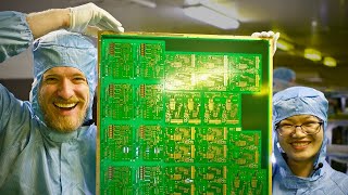
Walking Through a Big PCB Factory in China | JLCPCB

Вставка
- Опубліковано 26 чер 2024
- Watch how PCB is manufactured and how boards are assembled. Thank you very much to JLC for helping me to create this video.
Links:
- JLCPCB: jlcpcb.com/
- FEDEVEL online courses: www.fedevel.com/courses
Chapters:
00:00 What is this video about
00:14 Raw material cut to panels
01:21 Cleaning PCB
02:59 Photosensitive film applied (Building layers L2 & L3)
03:56 Exposing L2, L3
05:39 Developing L2, L3
06:36 Etching L2, L3
07:27 Removing photosensitive layer
08:01 AOI - Automated Optical Inspection
08:55 Making copper rougher
10:43 Adding prepreg
11:19 Adding copper sheets - Top and Bottom layer (L1, L4)
13:01 Baking PCBs, oven room
14:54 Splitting to two panels again
17:06 Adding aluminum sheet
17:30 Drilling
19:39 Plating
20:52 Electroless plating
24:18 Electroplating
27:35 Applying photosensitive film on L1 and L4
28:19 Exposing L1, L4
30:15 Developing L1, L4
31:24 Applying tin layer
33:30 Removing photosensitive layer from L1, L4
34:38 Etching L21 L4
34:50 Removing tin layer
35:48 AOI - Automated Optical Inspection
36:35 Optional electrical testing
37:53 Adding solder mask color
40:06 Exposing solder mask
41:55 Developing solder mask
43:27 Making silkscreen
47:23 Gold plating
49:54 Optical inspection, fixing, measuring
51:08 Electrical test
52:13 Milling - Removing PCB from big panel
53:36 V-Score
55:34 Packing PCB
56:32 Board Assembly
57:34 Inserting components into feeders
58:51 Stencil & Paste
59:18 Setting up component placement
59:51 Checking placement with AOI
1:00:42 Soldering - Going to owen
1:01:15 Checking after soldering
1:01:56 Assembling a board
1:04:30 3D printing
1:07:13 Done. Packing and shipping - Наука та технологія


I really hope this helps everyone who is designing PCBs. PS: Correction, 20um is 0.8mil, not 8mil. Thx @rb8049 for pointing it out.
😊
hey, at 8:16, those PCBs are designed by me for a client in Germany. I recongized the layout, what a small small world we live in
That's because China steals everything. There's an interesting video on Chinese fake Op Amps.
Unlikely
É meu projeto
WOW :-)
@@DavidUrulski-wq9de Given most of Robert's audience is professional engineers or students, it's quite plausible.
I spent 16 years working in a PCB fab shop and always find it hard to explain the steps needed to manufacture a PCB to my fellow designers. This is a great reference I will be sharing with them. Thanks for creating this video!
How does the scale of this fab compare to fabs in other countries?
@BobCollins42 I have visited a number of PCB manufacturers, JLCPCB was far the biggest one and the most automated one.
Is there any openings in your company to join as an employee?
Amazing detail, I like it how you kept your camera glued to the line all the way from start to finish. JLCPCB is truly one of the most important companies in PCB prototyping due to their very reasonable small batch PCBA pricing.
I use JLCPCB a lot for my circuits, and it's great to see this incredible manufacturing plant from the inside. What marvels of engineering! It's just fabulous. Now I understand better why my PCBs are always so beautiful and magical when I receive them :-) Thank you for this report and all the explanations. Very interesting.
Wow , What automation ! Material handling....Super. Thank you for sharing
Thank you Robert. You did an excellent job filming and explaining the process. It’s a very impressive operation.
Holy shit! Multilayer PCB construction is a real marvel of engineering. Makes you appreciate a bit more all the work that goes into this just to have all the electronics that we enjoy today.
This is really impressive. I've been to pcb factories before, but the scale of this factory as seen in the drilling room is just crazy. What i think is quite impressive too is that they have to know exactiy what steps each panel needs to go thru, and have the right data applied at every step so it all fits back together in the end with the correct stackup. And then once they are cut from the big panels, the correct pcbs get put togehter and actually go to the customer that placed to order or get to the assembly and soldering process. I would also like to know how much of the factory is actually just processing of clean air, and all the water/cemical treatment they have do in the background to keep the production lines running consistently.
I live near a factory. Every time I need a PCB for DIY, I specify a production base. Usually you can get the PCB the next day. Thanks for the video that allowed me to see the inside of the factory.
@ 41:33 I was already wondering how they are able to do these small designs for these low prices, but this shows what I was already expecting.
They basically combine just multiple designs into one big board and than remove and sort them accordingly.
I noticed that some manufactures in Europe still do everything by separate order, but I think this is a much smarter way of doing this.
In a way, the scale and size of JLCs factory combined with their automation is precisely how they manage to keep the PCBs so affordable! By standardizing on a limited number of stackups and being able to batch all these orders, they can get huge scale and spread those cost efficiencies over all PCBs.
This video (and your channel!) is a gem.
The scale is impressive, it makes sense how they can make them so affordable.
in china, JLC's PCB in 10cm*10cm is free(including postage), dont know the situation in other country.amazing company😚.
Amazing, just placed another order with them the other day. They have the GIFs on the site but it really doesn't do it justice compared to this video. Amazing, thanks for sharing :)
Thanks for this wonderful video showing incredible and how complex process it is.
Great show. Thank you very much for your work.
Excellent video! JLCPCB is the best!
Nice! I will be ordering mine from JLC soon. Thanks for the intuitive video
The drill proses sims to drill several pcb ones, that is why the minimum pcb you can order is 5 ....
exactly what I thought when I saw it
WOW! Just imagine the insane amount of investments needed to do this PCBs, now I know why "Scale" is what makes possible to have 5 PCBs for 2$... it is sad to think at small local PCBs fabricators who simply can't compete with price, Years ago, I had manufactured many little PCBs from a PCB manufacturer here in Italy, but after some years of not designing new PCBs, I discovered my usual PCB manufacturer was out of business, that was sad, I was happy with them. After, I decided to try JLCPCB and still prefer them now, all the PCBs I have had manufactured by them are very good.
Hey Robert, thank you very much for this video. Makes me more confident on using JLCPCB services. It makes it even more unbelievable that they can maintain their price range.
Wow this is really stunning. It's crazy to me how we can pay a small amount of money to have our own custom PCBs created in this huge process that involves so many delicate steps. Thank you for the great video and explanation of the whole process.
Pre-preg is not just an insulator, it's a hot-melt glue sheet that bonds all of the layers together. In the UK, the layers are aligned with pins on a Steel plate, with holes punched into the layers. alignment rings are etched on each layerto check the alignment later using an X-ray machine. That takes the best fit and drills location pins that provide the alignment for subsequent drilling operations. I don't think there are any plants in the UK that have this level of automation. the industry was decimated by foreign competition to the point where all that's left is a shell of the original industry. High value and Military work or very fast turnround business is all that's left. I've used JLCPCB, and can't fault them.
I have ordered some PCB and the quality is very good. The web and the process is very easy well explained. But what is most incredible is that for just 3.9€ (shipping included) I get the PCBs at my door. I think that just the blue cartoon box would cost more in the shop around the corner.
Because the scale of JLCPCB is very large, the manufacturing cost of their 5-piece PCB is close to 0, so the 3.9 euros are almost all shipping costs
Very nice video. I like that you took the time to show a lot of details. Other youtube channels have done something similar, but they crunch it into a 10min video, and leave tons of details out. Glad you made a 1h+ long video.
Amazing, many thanks for this insight!
Super informative and learning video. Thanks.
This factory is a good place for Big data or data warehouse for A.I training of PCB design for China. They have a lot of PCB design from around the world.
Incredible! Now I know all the work behind my mere hobby boards. I subscribed to your channel.
Here copper ball is used as an anode in the copper Electroplating.
There were multiple Surface finishes such as,
1.Hot Air Solder levelling
2.Electroless nickel Immersion Gold
Thank you! I've been using JLCPCB for years and have really enjoyed this wee look behind the scenes!
Just amazing!
Thank you sir for sharing this video
wow that resin printing with sanding is something I will try I think!
This is the factory I use to make bespoke vintage legacy PCBs I design or remaster with a variety of software. Of course I can make my own at home with advanced UV photolithography, but it's nice to have solder mask, silkscreen and precise hole drilling so I am happy to use JLCPCB for all of my light production needs.
How do you "remaster" PCBs? Asking because I find the wording among fellow legacy electronic enthusiasts always quite curious.
@@1337Shockwav3 Etching.
18:16 this is why you can only order multiples of 5 PCBs!
That makes perfect sense. Great eye!
Why? Aren't there 6 drilling machines? Am i missing something?
interesting topic, great video quality, no commentary needed during the 80% video.
Awesome...cheers.
what a beautifull pcb factory.
Great movie ! I want more :D
Amazing !
Thanks it is a super excellent travel for electronic live.
Really brilliant company
It's nice to see one of my PCB created from there 😊
Amazing.
Very high professional PCB manufacturer.
At 35:58 where you say its an automated inspection - is actually a process called reflow, where the panel is passed across flux/IR heaters/wash which melts the tin plating and causes it to flow-out. Noter the difference when they come out of this step and both sides of the panel are now "shiny silver"
The Chinese have worked quite hard in the last 60 years to reach where they are now in terms of being self sufficient. Inspite of whatever flaws exist in the Chinese society and government, this is still truly remarkeable!
What flows...china is good...do not implant your ideologies in other societies
Nice video
I didn't expect that to produce my PCBs is as complex as this. Thank you JLCPCB now I am so grateful and realize that my PCB is so cheap yet at best quality. What more surprising is we can order as minimum quantity as 10 pcs only. Amazing.
58:50 - to the right of Robert's PCB, there's a weird-shaped PCB with what looks like an ESP32 or similar RF module doing exactly what they should not (as per another video of Robert's): place the module with the antenna in the middle of the board!!
:)
I designed 2 custom boards and had them manufactured at JLCPCB. I can confirm they are good. Also if any of my colleagues and friends see this comment.
Hi guys :D
This reminds me I still need to pony up the money to complete my order!
exente el proceso de fabricación
The PCB drilling machines use Air Bearing Spindles that typically go up to 250,000RPM, yes, a quarter of a million. You need this for the very small holes else you can't drill them quickly enough. When I was involved in the industry, 0.2mm was the smallest size, but today it's half that. This is why panels are only drilled one at a time. Years ago we used to drill through four panels at a time, when the smallest holes were 0.7mm
Awesome video. This kind of setup seems like AGI will have no problem taking over. I noticed one person who was manually moving boards at a 90 degree angle, while peeling film off each panel moving from applying the UV mask into the chemical area. This person will be a god to the AGI. Either that or she will be replaced by yet another robot arm.
Really cool journey to see what is inside the JLCPCB, I am going to order some 3D models from JLCPCB, thank you
Several of my PCBs have gone this way. 🙂
I see they apply conformal coating but on the website I cannot find a single mention about it, how can you request it?
Modern PC Motherboards are up to 12 layers, it's amazing to see the process
I heard that some phone uses 20-layer PCBs
At 25:27 the cooper balls are being used as anodes to transfer cooper to the pcb during this process I believe.
主流的方法是贴上一张感光材料进行蚀刻。大约40年前,感光材料是通过丝网印刷来应用的。
Does anyone know how many little roller wheels and gears are in the factory?
I've been using a number of services and well, their results from JLC really convincing. So far I've only had one minor messup (order number not being placed in the location I defined, to which I also never got a reply by support). On the other hand I've had PCBs with defects (shorts) or taking a serious premium for sub par quality (and not being produced locally, only mentioned once in the smallprint). The other major chinese PCB manufacturer also is beyond annoying by hijacking pretty much every hobbyist channel on youtube as a sponsor *and* their "shared design" endorsing people to profit off stolen designs.
Wow 🎉
Missing Solder masking & Slikscreen process😂😂😂😂
2 bucks for 5 pcbs is still wild
You must have resistive and semiconductor nm layer fabrication for multi layer components.
4:21 how long does the exposure actually last?
This is really fascinating. I'm interested in the manufacturing machines. I wonder if they are engineered and built in house by JLCPCB or if they are made by a different company.
in the oven part, minute 13, they only put in the oven, and just with the temperature the layers get toguether? not put presure in the layers??
I thought that the balls are to prevent 'Evaporation' not sure now ! Great to see where my boards are made....cheers.
Wow, no wonder their prices are so competitive on world stage.
视频中没有出现半固化片前铜面的表面处理部分吗?
"i dont know what this is doing"
"try to guess what is going to be next"
"Uhhhhh some sort of cleaning....I guess....uhhh...."
Plus comments are astroturfing. Most of them spelling out the entire company name are new accounts, no profile pictures, and poor English skills. Just embarrassing.
Very nice video👌, from a "real pcb" designer.❤👍👍Still not done watching in full(more interested in the testing and assembly parts and other services). Some comment for the aluminum foils during drilling: They are placed to reduce burrs as the drill makes entry. It is critical to the thruhole creation process that follows it, to have a continuous conductive path to the via walls, to create uniform and reliable plating inside holes.
Also, drilling bits are cheaper to use and refurbish. Instead of using a hundred drill bits with an automatic tool changer, it could be done with very few endmills and trochoidal milling. But endmills are expensive(upto 10X) and cannot be easily refurbished. Just some insights.
Hey, how did you create the spinning PCB Video at the beginning of the video?
it's spinning on a wire and the wire is removed in postproduction
我想看看数控钻孔后的化学镀孔。
ironically i had to watch a pcbway ad during the video
I also ordered pcb from JLC when I was I China, very affordable price.
Do they prepare a plan according to the client's request?
👌👌
How did JLC expose the photoresists? I didn't see them using the clear mask overlays, how are they doing this now days? Lasers? Scanning UV LED line array? LCD matrix?
All Great, but, at 1:05:28 you can see that they wear Fake anti-static bracelets "wireless" :) 😉
Ah yes, I've found the know all idiot of this comment section
I work in this kind of factory 30 years ago. Not much change.
I was hoping to see one of my orders going through PCBA at the moment 🤣🤣
:D BTW, this was recorded in September.
@@RobertFeranecI also have a order in PCBA at the moment that’s taking a little longer than expected, and of course the first though that popped into my mind when I saw this video was “Robert was probably holding everything up”
@@lynestelles3899 :D
❤❤❤❤
Hi Robert, im curios about the vias process, May be i lost it in the video. Of course .. great video
this will help you: ua-cam.com/video/ukfsupePkOM/v-deo.html
pcb is assembly with the 3d printed case, or send separately?? thank you
When I was ordering the last time, they had to send them separately (I think the main reason was customs). I am not sure how it is now.
Wonder why we can't have a factory like this in the US making PCBs for cheap. I would bet none of those fabrication tools are made in China.
Also wonder if those lithography steps used masks when exposing the photosensitive material or if its direct write. I would guess direct write to save money and time on masks, but that was SUPER fast for exposing that massive area.
除非能够自动传输从 NC 机器出来的电路板,否则布局可能会导致良率下降。
Hey Robert , I am completley new in this field of design , the biggest issue I am facing how to create circuit design , datasheet contain so many things for each component so it became difficult to understand what point to consider what to not , how should I approach , I am complete begineer in thiss field ( where to use pull up resistor , where to use coupling/decoupling capacitor , wht should be there value , should be they be in multiple numbers or not ????? Alot of confusions , Can you please help me out how should i approach taking baby step for designing!!!!
please, to ask questions, the best is to use our discord here: discord.gg/8a8dUcHmrx
Y estas fabricas existen en Europa?
Pregunto.
We love JLCPCB. Is there anyone who still doesn't know JLCPCB?
These comments sound like the epitome of an astroturfing campaign.
Why is the guy at the end visually checking the circuit? They have thousands of layouts coming out per hour maybe.
Sweet suit 😅
JLCPCB have good quality. Buuuut.... its a pain in the butt to order stencils. They allocate one tracking number but send 2 different packages. I soooo wish they would strap them together. Courier only sends the pcbs and declares the stencil package as unknown. Lost a lot of dollas and stencils. Gonna try PCBWay next to see if they get it right. Sad to leave JLCPCB! (Airfreight to Africa takes about 3 month - if the local post office doesn't loose your parcel)
In my orders, milling is the first step, but not in this video. It's also interesting to see they feed cut tapes instead reels to pnp machine. I am also surprised they are still using pneumatic feeders.
What is the size of the panels we are seeing?
I don't know the exact size they use