Very helpful and informative videos. To the point, all things covered, excellent images and video quality. Literally I prepared for my exam in couple of hours from you the whole content of semester. Thanks bro, Sir ❤
For more info, check these other useful videos: 1) Latch and Flip-Flop Explained ua-cam.com/video/LTtuYeSmJ2g/v-deo.html 2) SR Latch and Gated SR Latch ua-cam.com/video/xONsaRVYQmA/v-deo.html 3) Introduction to Sequential Circuits: ua-cam.com/video/fLN1YOmuAr8/v-deo.html 4) Digital Electronics (Playlist): bit.ly/31gBwMa Link for the Multisim Simulation : bit.ly/3tGWBuL
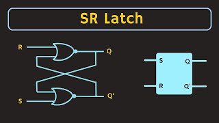
Its the only place where Gated SR latch is not called a Flip flop , all other places on either youtube or coaching classes call this gated latch a flip flop......... I don't know why people refrain from analyzing using timing diagram, I was so disheartened that such a basic thing is covered wrongly in all places..😢
Sir i have a doubt, from the positive edge triggered SR flip flop,in the case where S=1 and R=1 why is the output of the AND gate 1 during clock transition period, and why is it becoming 0 just after clock transition, as just after clock transition, clock input would be 1, so 1 in both inputs of AND gate should be 1 na
S and R is present state right(that's what my understanding), then you have to copy the values of S and R in present state right, but you are making everything as 0 and 1 how? Just tell me how we are getting the present state values. I know about the first three rows 8:34 in present state, explain about the last 2 rows for present state.
Please check it once again, when S= 1 and R = 0 then flip-flop gets set to 1. Qn+1 is 1. (The fourth row) Regarding your second question, in the flip-flop design we are getting two complementary outputs. Some times Q' is also used in the circuits. For example, when you design a sequential circuits using Flip-flops then sometimes Q' output is connected to the next stage of the circuit (just to save one inverter)
S= 1 and R = 1 input is prohibited in the SR latch/flip-flop. Because when both inputs are 1, then Q and Q' is 0 at the same time at the rising edge. And after the rising edge, depending on the propagation delay, the output (Q and Q') will be either (1,0) or (0,1). I have already explained that from 8:33 onwards. Please watch it once again. You will get it.


ECE saviour 🙌🙏
Thnks a lot sir
Very helpful and informative videos.
To the point, all things covered, excellent images and video quality. Literally I prepared for my exam in couple of hours from you the whole content of semester.
Thanks bro, Sir ❤
For more info, check these other useful videos:
1) Latch and Flip-Flop Explained
ua-cam.com/video/LTtuYeSmJ2g/v-deo.html
2) SR Latch and Gated SR Latch
ua-cam.com/video/xONsaRVYQmA/v-deo.html
3) Introduction to Sequential Circuits:
ua-cam.com/video/fLN1YOmuAr8/v-deo.html
4) Digital Electronics (Playlist):
bit.ly/31gBwMa
Link for the Multisim Simulation :
bit.ly/3tGWBuL
ALWAYS GIVING SOME THING SPECIAL, KEEP IT UP
You are a life saver 🙌❤️
Its the only place where Gated SR latch is not called a Flip flop , all other places on either youtube or coaching classes call this gated latch a flip flop......... I don't know why people refrain from analyzing using timing diagram, I was so disheartened that such a basic thing is covered wrongly in all places..😢
Exactly 💯 ture
great lecture sir
thankyou very much
Sir i have a doubt, from the positive edge triggered SR flip flop,in the case where S=1 and R=1 why is the output of the AND gate 1 during clock transition period, and why is it becoming 0 just after clock transition, as just after clock transition, clock input would be 1, so 1 in both inputs of AND gate should be 1 na
It is 1 for a short period of time because of delay see 18:38
S and R is present state right(that's what my understanding), then you have to copy the values of S and R in present state right, but you are making everything as 0 and 1 how?
Just tell me how we are getting the present state values.
I know about the first three rows 8:34 in present state, explain about the last 2 rows for present state.
Understood myself sorry pal ✌️💪
sir please reply why at 8:20 the flip flop get reset to 0 0 if S is 1 and R is 0., and why we measure Q and not Q'. Please reply.
Please check it once again, when S= 1 and R = 0 then flip-flop gets set to 1. Qn+1 is 1. (The fourth row)
Regarding your second question, in the flip-flop design we are getting two complementary outputs. Some times Q' is also used in the circuits. For example, when you design a sequential circuits using Flip-flops then sometimes Q' output is connected to the next stage of the circuit (just to save one inverter)
What a explanation... 🎉
Man you are amazing
2:12 why the output of this xor gate is equal to 0? Maybe previous stage is 0. I didn't undarstate that.
Here, just for explaining, the initial state of the XOR gate is assumed as 0.
Sir are you mr. Mohammed shanawaz sir from heritage institute of technology?sir please tell me. I am eagerly waiting for your answer.
Please check the about section of the channel. You will get it.
bruh app kon se year se ho ??
Sir please also upload video on gated D-latch
Please check this video:
ua-cam.com/video/EILb-DrYr8A/v-deo.html
@@ALLABOUTELECTRONICS I have seen .Thank you bhaiya . You are awesome
Sir how sr flip flop using nand gate is different from this Nor gate sr flip flop?
Sir where are the videos of JK , T and D flipflop.
It will be covered very soon.
when the present state is 0 1 and the input changed to 1 1 now what is the next state of the sr latch or flip flop when enable is 1
S= 1 and R = 1 input is prohibited in the SR latch/flip-flop. Because when both inputs are 1, then Q and Q' is 0 at the same time at the rising edge. And after the rising edge, depending on the propagation delay, the output (Q and Q') will be either (1,0) or (0,1). I have already explained that from 8:33 onwards. Please watch it once again. You will get it.
yes sir i got it thank you so much@@ALLABOUTELECTRONICS
i got it sir thank u so much@@ALLABOUTELECTRONICS
11:59
Why are you talking like a robot? You always end each of your statements with the same tone. Not trying to be rude, just found it distracting.
❤
Ur teaching is awesome bt can you use Hindi language also?????
Sir kmap was wrong
Would you please mention where you are referring ?
In characteristic eq of SR FLIP FLPO
@@shashankkumar7141 Its seems alright !! And the characteristic equation is also alright !! Just wanted to know, why do you feel its wrong !!
@@ALLABOUTELECTRONICS No sir, it's correct. 👍