
Вставка
- Опубліковано 2 сер 2024
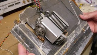
- This video shows the reverse engineering of the demodulator module of a vintage gyro subsystem GR 10A-1 manufactured in 1965 and designed for an Atlas Launch Vehicle.
00:00 - Intro
01:26 - X-ray analysis using XYLON Cheeta EVO
04:07 - Preamplifier
07:53 - Complete schematic diagram
08:39 - Modulator
Merci à la société Inovelec pour avoir consacré un peu de temps à l'inspection aux rayons X de ce module, ce qui m'a permis d'effectuer la rétroingénierie de celui-ci.
inovelec-groupe.com/
Other episodes:
• LDM #362: Atlas Launch...
• LDM #363: Atlas launch... - Наука та технологія


hello le labo de michel nplis 2parts amazing video may from aargeentina nice vidio thank yu brooooooo
amazing work! thank you
Beautiful the X-ray
Great work! Nice to see it !
Did the Russian proton-M with the backwards-installed gyro that did a back flip have such helpful text written on the box?
Not that an idiot would let that stop them.
Nice work as always 😊
Bacana essa fotografia em raio x
Excellent.
Je ne pense pas que ce soit une tomographie mais plutôt un CT ou un CBCT. En tout cas, un bel appareil à haute résolution!
Great X-ray photos. I'm curious to know how you found the component values.
I was waiting for this question... Actually I succeeded after one day of hard work to remove the potting below the pcb, on the solder side. Therefore it was possible to measure the value of some parts.
👌👌👌👍👍👍..... Greetings....!!
Very interesting, thank you for posting! I saw the comment below about part values - may I ask how you removed the compound? Physical force or did you use any chemicals? Heat? Another question - there was some misalignment for the xray image - was it scanned in tiles and then reassembled, for higher resolution perhaps? The capacitor internals match solid tantalum designs, which makes sense for the application.
I have used a hot air gun, set to 500°C. The compound was less hard and it was possible to remove it in small pieces using a screwdriver. It was impossible to do the same on the component side because of the thickness of the compound and the parts.
Concerning the X-ray a total of six pictures were taken, the module was too large for a single shot. Image area was maximum, the resolution of the picture can be much better with smaller areas. After I have reassembled the images to get a single one. It was impossible to have a perfect alignment everywhere.
@@lelabodemichel5162 Thank you for the de-potting information. We all hope for a magic solution to this, but it never exists, does it. At least it was a partial success. Regarding stitching of images, it's always possible to use "grid warp" tools to align tile edges manually. For GIMP it's the W shortcut, and Photoshop has a grid warp tool as well in the transform section. There are also dedicated open-source tools like Hugin to do all this automatically.
@@oriole8789 well, actually there are specific solvants to remove the potting compound, they work very well but they also damage the board (more or less), so in most cases it wont be functional after the process, you will however be able to read most parts mpn and measure values on the parts which have not been damaged. The solvant mostly eats the PCB FR4, soldermask etc.
Это использует дифференциальные трансформаторы в качестве датчика ?