CMOS Tech: NMOS and PMOS Transistors in CMOS Inverter (3-D View)

Вставка
- Опубліковано 8 вер 2024
- CMOS technology uses both NMOS and PMOS transistors fabricated on the same silicon chip. The PMOS transistor is connected between the power supply and the output, and the NMOS transistor is connected between the output and ground. The NMOS and PMOS transistor gates are connected, forming the input of the inverter.
In the CMOS inverter and other CMOS logic functions, the output is connected through one or more transistors to either the power supply or ground. There is never a path from the power supply to ground (a short-circuit path). Furthermore, there is no current flow in the steady state, as the logic gate inputs are implemented as transistor gates, which are insulated from the source and drain terminals of the transistor.
Current flows only during switching from one state to another. Therefore, energy consumption depends on how often switching occurs and whether the logic switches in on each clock edge. Current flows only to charge or discharge parasitic capacitance in the circuit.
The logic gate output must always be pulled high to the supply voltage or pulled low to ground, and never allowed to float. A floating output results in an unknown intermediate voltage a the inputs of the gates downstream. This can cause both the PMOS and NMOS of transistors to be partially turned on, providing a short-circuit path from power to ground. To prevent this, the gate output must be connected through one or more transistors to either the power supply or ground.
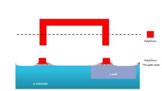
Transistors are built using N-type and P-type silicon. In N-type silicon, a small fraction of the silicon atoms are replaced by an impurity such as phosphorus that has one more electron in its outer shell than silicon. A phosphorus atom easily gives up its extra electron, creating a negatively charged mobile carrier (electron) and an immobile ionized atom (phosphorus). N-type silicon can conduct electricity by means of its mobile electrons.
In P-type silicon, a small fraction of the silicon atoms are replaced by an impurity such as boron that has one fewer electron in its outer shell than silicon. A boron atom easily accepts an extra electron from a neighboring silicon atom, resulting in an immobile ionized atom (boron) and a positively charged silicon atom with an electron shortage. The missing electron is called a hole. A hole works just like a positively charged mobile particle because an electron from a neighboring silicon atom can jump into the hole, creating a new hole. P-type silicon can conduct electricity by means of its mobile holes.
Next video: CMOS Inverter Model Using Light Switches
• CMOS Inverter Model Us...
For more information, see the free textbook "Modern Semiconductor Devices for Integrated Circuits" by Chenming Hu: www.chu.berkel...
Silicon & diamond unit cell atomic model, wafer/crystal orientation, Miller indices (100) (111)
• Silicon & diamond unit...