Copper metalization with a diode laser

Вставка
- Опубліковано 14 чер 2024
- CONSIDER SUBSCRIBING 🥰
☕Buy me a coffee? www.buymeacoffee.com/Breaking...
🔬Or Patreon if that's your jam: / breakingtaps
📢Twitter: / breakingtaps
💻Discord: / discord
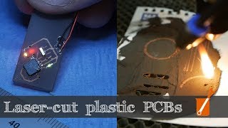
Three laser experiments today: laser-induced electroless copper plating, laser-assisted electroplating on stainless steel, and laser-induced chemical liquid phase deposition onto glass. Whoo! I'm using a "20W" 450nm blue laser etching machine for these experiments, and while a bigger or pulsed laser would work better, it did a pretty ok job.
0:00 Intro
1:03 Laser-induced electroplating
5:37 Effect of insulators
6:22 Stainless Steel deposition
10:15 Laser-induced Chemical Liquid phase Deposition
Al‐Sufi, A. K., et al. "Laser induced copper plating." Journal of Applied Physics 54.6 (1983): 3629-3631.
Gupta, Ram Kishor, et al. "Maskless copper electroplating on stainless steel using DPSS green laser." Surface Engineering 34.6 (2018): 446-453.
Manshina, A., et al. "Laser-assisted metal deposition from CuSO4-based electrolyte solution." Laser Physics Letters 4.2 (2006): 163. - Наука та технологія


Awesome! I may have to 'borrow' this recipe for some ceramic PCBs 😏
Goodluck! Let me know if you have questions or run into issues. Fair warning, the recipe I ended up was mainly a function of the chemicals I had on hand at the time :) There are definitely better recipes in the literature. In particular, CuCl is supposed to give more conductive deposits, and someone else here in the comments mentioned a paper showing Xylitol doing much better than EtOH or formaldehyde. "laser-induced chemical liquid-phase deposition" (LCLD) seems to be the right keyword to start pulling up most of the literature.
Oh, and one last disclaimer: I had a tough time soldering to it, might need to use a reflow oven and paste... or some kind of exotic solder. Or maybe just better cleaning than I did, which was next to none :)
Cheers for stopping by, really enjoy your channel :)
Can't wait
Robert Murray-Smith - ua-cam.com/users/RobertMurraySmith - has made a conductive ink that might be excellent for making plated through holes in regular pcb's. anyways
If this method Cu metalization doesn't work (very interesting to me too), perhaps coating the ceramics in ink, electroplating it with copper and developing it normally with photoresist+etch might work :ø)
Edit: Since the ink is conductive, it might also be required to remove it, and I doubt it will be etched away - perhaps blasting it with a laser so it evaporates, like removing an ink tattoo?
@@BreakingTaps did you mean xylene or does the literature really use Xylitol? Not trying to be a dick here i'm genuinely interested in the answer because that would be super weird.
@@Amasarac Haha, no problem. Yep, really xylitol :) here's a quote from one of the papers: "Multiatomic alcohols, sorbitol, xylitol, and
glycerol, are shown to be effective reducing agents for performing LCLD at glass-ceramic surfaces" www.researchgate.net/profile/Ilya_Tumkin2/publication/269319964_Laser-Induced_Copper_Deposition_with_Weak_Reducing_Agents/links/55dc513608aed6a199ad097e/Laser-Induced-Copper-Deposition-with-Weak-Reducing-Agents.pdf
This is getting me applied science, tech ingredients or thought emporium vibes.
That means a lot to me, I'm a big fan of all three of those channels! Thanks!
Tech ingredients and thought emporium are two of my top applied science channels. I definitely noticed similarity in quality of learning on all 3!
Let us pray he is a _Holographic chocolate and Banana brandy-sort of scientist!_
This is a really good technique, I'm quite impressed. Just a warning, with experience since we manufacture the L-Cheapo line of diode lasers: this will kill your laser VERY quickly with direct reflection! If you wish to avoid destroying your equipment, you need to set the laser at an angle to the workpiece (even a few degrees will do) so it doesn't fire right back into the diode!
Note that because you are working with a liquid and gravity is in play, setting the workpiece at an angle will reduce reflections (due to the copper) but not completely eliminate them (due to the surface of the liquid). Better to angle the laser.
Oh, that's a good tip! Will start putting a slight angle on the diode from now on
Laser specs?
@@donaldviszneki8251 Ours is the L-Cheapo MK7.
So it's basically the magneto optical affect applied to electroplating. Genius.
This is awesome, you should try it on FR4 circuit board material.
I'm 4 videos in on your channel, subbed after 1st vid.
Woo! Thanks for watching :)
This is the first video of yours I've seen, and I'm getting massive applied science channel vibes. Which is a huge component BTW. Loved this video
For cheap sapphire blanks, look at replacement watch crystals. Should cost $4 for a single 40mm blank.
Genius! Thanks for the tip, will look into grabbing a few
if the sapphire is clear isnt it just corundum?
the blue color from impurities is what makes it sapphire. chromium impurities make it ruby.
like the difference between iron and steel is carbon impurities as well as other metal making steel alloys.
@@darkshadowsx5949 I've heard people say "saphire" regardless of what impurities are in it, including what most people would call ruby.
@@darkshadowsx5949 natural sapphires can be almost any color. Impurities are titanium and iron oxide. The carbon in steel isn’t “impurity,” the trace sulfur, silicon, etc.. are.
So, I have been searching and talking to myself in front of my phone, recently, in search of a rapid prototyping process for the development of PCBs and the potential use of aluminum nitride as a PCB substrate for high performance applications.
I was thinking of vacuum chambers and particle beams - but this seems infinitely more reasonable. Even I need thicker films than what would be practical to 'print' using something like this, I could use the initial layer as a seed for a more traditional electroplating process.
The spooky algorithm in the machine can occasionally be quite helpful.
Haha "spooky algorithm in the machine" indeed, feels like it's read my mind on occasion as well and served up exactly what I needed.
So caveat to this process, the recipe seems to have a big impact on how electrically conductive (and robust) the traces are. There is another comment here somewhere showing a paper which compared different components and xylitol + copper chloride seemed to be the winner. I saw a different paper that compared the durability of the traces, and unfortunately don't remember the details but some recipes stood up to ultrasonic cleaning better than others. Which would probably be important to get the crud off the top and use it as a seed layer.
But yeah, otherwise it seems to be a really useful technique as long as your material is transparent! On a more recent project I cheated and used a fiber laser to ablate away a pattern from some adhesive copper tape: ua-cam.com/users/postUgyT5bl94pSSUmr7HI14AaABCQ Sorta dirty hack, but it worked :)
There are some interesting improvements for this in
Robert Murray-Smith's channel in his video "993 'Printing' Copper With A Laser". He is solidifying the copper from a dried version of this solution. Seems much simpler if it works just so easily.
Just saw that, very cool! I pinned a comment on this video so other folks would see it... definitely an easier and less-fiddly technique. Might give it a shot myself! :)
I definitely prefer this "Applied Science"-type experimental content rather than "This Old Tony"-type machining content.
Great to hear! I was originally nervous pivoting from the machining-stuff to science-stuff, but I enjoy the science more and frankly, I'll never be a very good machinist relative to others on YT. Or as funny as ToT :)
@@BreakingTaps I actually really like your humour because it's very low-key and humble. So it does not distract attention from the actual content of the video. Sometimes after watching ToT I still don't understand what he was actually doing lol.
I love this side project. I've never heard of this before. Very interesting. Thanks.
Funny, it's seems similar to moon dust gaining a charge , and levitating, when hit by sunlight. More or less.
I love this stuff! Thanks so much. Plus this applied stuff really helps me better understand o-chem terms like 'ligand' and 'chelation' better.
Very Applied Science feel to this video. Wonder if you can build a circuit on a transparent substrate using this technique.
Thanks! I've gotten a bunch of questions about that, will test it out! Main issue is soldering I think... a quick test with a solder iron didn't work well. I've ordered some solder paste to see if more even heat in an oven works better.
@@BreakingTaps Run the circuit board you have fabricated through a tinning bath before soldering? ua-cam.com/video/Hsw3lOnHaas/v-deo.html
Oh, neat! Didn't realize that was easily done... will look into that. I bet that would help considerably
Cool demonstration. Well done.
I love a bit of chemistry in between my machining in my own workshop... so this is great.
Brilliant. Thank you
def mynew favourite channel thank you for the great content
sooo, i've discovered your channel and i am now very happy since it's exactly what i'm aiming to work in, cool material science
Love your channel. Amazing videos so inspiring. Thanks a lot
Truly awesome! Thank you!
That's badass! Good work man!
Yes! This was an awesome project, keep them coming :D
Never seen anything like this. Thanks!
This is awesome, great job.
This is super awesome.
Indeed it would be great for circuits on fancy surfaces😊
love the thinking outside the box. was just thinking about if someone has tried it with a co2 laser, certainly the slide one would have to work on the surface not the obverse due to the low transmission of the wavelength in glass.
Awesome, thanks!
wow this looks like it has a huge use case in additive manufacturing and could be a gamechanger
Great vid thanks !
Just stumbled on your channel and subbed for the great content
So cool. Well done!
-Ken
Best stuff I saw in a while.
Thanks!
pretty cool letter heads/business cards .. - whatever dazzles people , catches their eye ... "sell the sizzle ", .. woos and wows gets the cows ..
Cool stuff! Thanks for sharing =D
Great job, excellent video! Perfect for coping with applied science withdrawal symptoms.
Considering the amount of variables it looks like this could be fine tuned for even better results. Have you found any papers using other metals with a similar technique?
Subscribed and looking forward to future experiments.
Thanks! I saw some papers that did this with Nickel as well, so I suspect it works with any of the normally platable metals (but don't have proof of that outside copper and nickel).
very good! Full support from Endurance lasers!!!
Thanks! Was actually just looking at your 532nm DPSS lasers. I keep finding a need for a pulsed, shorter wavelength. Will be in touch!
Huh, I might have to try this. I was wanting to etch circuits onto glass. This is way better than how I was going to do it.
Copper is very easily released from solution on more active metals such as zinc, aluminum, iron. This does not require additional energy sources, because that potential difference, which is given by the metal itself, placed in the electrolyte, is quite enough. After all, this is a school experiment, when an iron nail is dipped into a solution of copper sulfate, and after a while a layer of metallic copper appears on the nail, which, however, is very fragile and can be easily erased with a rag. That's why you got a fully copper-plated piece of stainless steel leaving it in the solution.
I found this video on my recommendations, you're video is as mush enjoyable a "applied science" video
Nice discovery, +1 sub
Woo, thanks! That's high compliment indeed, I'm a huge fan of Applied Science channel :) Cheers!
This channel is underrated!
Subbed
Excellent project. Really interesting. Very well done. Thank you for sharing.
I guess the guy from "TheThoughtImporium" might want to hear about this.
He is working on a neuron - electrical interface using an electrode matrix on a glass slide.
He was hunting for a good process for creating such structures on a glass slide and had teamed up with the guy from Applied Science.
The AS guy used a vapor deposition and chemical etching process. It worked, but that process was pretty hard to control and did not have a very good yeald.
Looks like your process would handle this much easier. Would be nice to see you two working together to get to see more of his fascinating neuron research.
..it has frickin' lasers, ofcourse we like!
" ......Subscribed!" Way cool mon'! TY for sharing. :D
Very interesting. The input photons seem to themselves radiate out some type of catalyst wave either the pressure wave or reflection of photons
Good content... add more please.
If you turn it all sideways, and lift the material out of the bath as you go, you could prevent the issue of the etching removing what you deposited.
Very interesting.
Never have I subscribed so fast
❤
The top spot mentioned at the beginning was the electroplating of lattices. Please come back and do those again. I really want to see you do this for larger pieces on a conveyor belts fdm printer.
very cool...
Wow, the glass deposition technique may be very useful for making brain cells substrates for bio computers very easily
In conventional electroplating alongside wetting agents in the solution we agitated the workpeice or the solution to avoid spots from hydrogen, it would be interesting to see if that will also help eliminate the spots in this process(If it won't mess with the lazer magic :D)
Nice work.
I thing about last part of video. When i've worked in electroplating plant we use surface wetters/surfactants (i don't know this mixture) for electroplating copper (ABS->digestion, activation, chemical plating of copper, electroplating copper, nickel until finaly chromium). Solution for copper paling have CuSO4 and H2SO4 and small amount (kg/tons) this wetters.
In electroplating copper this addition causes flat and shinny surface, free from bubbles and current instability.
I thing u have to buy glucose without any problems, this sometimes may replace use of formaldehyde (glucose is aldohexose) but it can reduce copper ion to Cu2O. Anyway - you can try it.
Awesome video! Here's an idea, can you use the microscope controller (the one with nanometre accuracy) and etch nano structures on the glass to create structural color like the butterfly wings. I know that laser wavelength is high, but I think Intel uses a process where they pass the laser through a drop of water and that makes it smaller. It seems like a complicated idea, but it would be so awesome if it works.
Great! I wonder how 405 nm will do. They are not DPSS, so their beam quality is much better, and the energy at those short wavelengths is quite a bit higher. Also, you could try citric acid in your last reaction. Its a great chelating agent for copper. Hopefully it will give it up when needed. All the best!
Interesting, will look into citric acid! And agreed, a 405nm would be interesting. I'm assembling a photolithography system using a 405nm (2W) laser for a different project... might have to shoot it at some of this copper sulfate solution and see what happens :)
Two years late, but this is so cool!
I suggest you try the electroplating to stainless steel again but with and without ultrasonic agitation. Also, double check the tube piece you squeeze in the vice, What material are the jaws made of? Try a repeat but with a barrier film between the jaws and the pipe. I'm wondering if the agitation from the laser localised heating is resonating on the metal piece, tension from a rubber band like a finger to a bell would work to determine this. I'm amazed by your work on this channel!
Yes please.
Very cool demonstration. One thing maybe to look at is testing with a UV laser or UV leds. Maybe the shorter wavelength/higher energy photons might produce some interesting effects.
yes, also trying X-rays to ionize it better.
For the copper on copper, what if you applied some "sub-threshold voltage" (i.e. not quite enough to start plating the whole sample) instead of doing it electroless? Seems like that would greatly reduce the etching effect, increase the plating rate, and let you go bigger and deeper.
Oh! Easier than magnetron sputtering!
It would interesting to use a lens to miniaturise the design - useful for making RF/microwave structures - e.g.filters!
Its like a welding pattern. Can you check the conductivity?
This is very good could you do Nickel plating with a laser
Another super awesome video! Have you tried plating LIG with this method?
Thanks! Not yet, but it's on the "things i'd like to try" list :) Ditto to electroplating the LIG... have some vague ideas that it could make for a neat catalyst material or something, assuming the plating process can get inside the pores some without filling in.
I might guess that the ripples in the 20x view are from the power rectification going into the diode laser, and how that filters out into the optical power output. e.g. if you don't have a large enough capacitor on the power supply, and you get a tiny 60Hz ripple or some other pattern, then that may not fully attenuate in the output. I wonder how well you could estimate the spacing between ripples, and if you could use the machine velocity to get the frequency
Could also be vibration from the motion system, which presumably uses stepper motors. If you are actually able to estimate the spacing, you could compare it against the linear distance from a single microstep. A neat looking pattern any which way!
Neat. I'm wondering if you could tune the frequency of the laser to the vibrational frequency of the copper atoms to heat them more effectively.
If you still have your samples from this video, put all of them under your AFM. It would be very interesting to see the height distribution before and after depositing copper on copper. And there is also the potential to use the AFM to watch the deposition in real time. Although, that could potentially use up a tip if you aren't careful about things and it ends up in solution. Using a tip in this way *could* be possible. Calibrating the tip with it already submerged could theoretically still allow it to function for a time. The conductivity of the solution would be the major hindrance as it would begin competing with the metal paths and that could quickly ruin the tip. There's really only one way to find out. All of that said, even the samples collected from this video would be very cool to see.
Oxidized formaldehyde is formic acid/formate (depending on pH, of course).
backyard scientist!
17:15 20x view: Looks like the bead from an automated welder.
When you scratched one side with your finger I was like "please don't do the other side" that gave me chills with the headset lol
Anti-ASMR 😂 (sorry about that!)
Your small rectangle of stainless may be austinitic stainless steel. A special variety that is essentially non-magnetic.
Also stainless comes in different grades and what makes stainless steel not rust is its other metal content so it might be stainless but have a higher copper content. I don't think a higher zinc content would do that but I'm not sure because I've never performed this experiment.
Controlling dissolved oxygen concentration will likely help with the quality and rate of deposition of copper in the essentially electroless bath.
Too high a concentration of dissolved oxygen can essentially re-etch the copper off. Too low would normally lead to a bath crashing out and plating out too easily onto anything and everything mildly catalytic, like dust, scratches in glass, existing copper, etc... Since you are using a weak bath that doesn't strongly want to plate out and the laser is forcing it, a very low DO concentration may actually work very well. Consider enclosing your experiment and purging the DO in the bath by bubbling nitrogen gas through.
polished stainless molds are used to electroform shapes that are easily removed...nickel is common.
Great video! Is the method could work on plastic sheets? I mean kapton, mylar, BOP?
I'm not sure to be honest, maybe? If they are clear it would _probably_ work but I'm not sure :)
Man, if that's procrastinating for you, you are doing good
Wow , plating so thick its textured. Hmm, print a coil and try to put ac threw it? Wonder if it could work over blue titanium plating .
Instead of glycerin im used sorbitol. By the way, any resin is good reducer, so you can make PCB just on any textolite. Source: Laser-induced chemical liquid phase deposition of copper from aqueous solutions without reducing agents Kochemirovsky,V A et al.
great video, I'm a bit late but what laser output power would be needed for an ablation process?
If you kept plating for a long time, can you make a 3d structure?
I wonder with the third process if you could "drag a bead" taking one slow pass a just build laterally on your first piece of copper once you get it started.
Could make pc boards using the glass as a cooling conducive surface
I plate copper over stainless regularly, in an artistic type setting. I first learned plating stainless is a thing when plating copper over various music strings that have SS cores (guitars, piano.) it doesn't fully "adhere" having to do with what elements are in your alloy, and their relationships to each other in the reactivity series. The copper is plating somewhat on some, and just cementing out on the other metal constituents. So therefore the other metals are contaminating your bath and may or may not precipitate out as slimes. Recently I plated a SS hip flask, and it was a success.
Oh, interesting! That makes sense, I guess some grains are more reactive to plating and then it just creeps over adjacent grains. Probably explains why the different SS samples I tried "plated" differently, being different SS alloys with different components. Neat! Thanks for the explanation!
@@BreakingTaps the first sample was probably contaminated by the cutting wheel used to cut the sample out of the larger piece.
It's not uncommon to see when someone doesn't have a dedicated stainless cutting wheel... Or even when the dust from cutting other metals lands on stainless.
Cool
man I will have to try this with the copper acetate solution I made for reacting with the aluminum on mylar thermal blankets to strip it and make aluminum acetate in the process (for another process to make quasicrystals of aluminum phosphate, while leaving copper oxide behind for making CCTO for "Join the technicians" channel Jeremiah's Antigravity research something he is doing to test given claims in various papers, in this instance the CCTO is for asymetrical high K low K dielectric material, with the CCTO being the high K material and hopefully being able to fire it in a kiln to shape here before mailing it.
I believe you should reason you may have had issues focusing the laser down when you add a larger amount of fluid in the petri dish because of the different refraction angle in the liquid medium. I did some experimentation with different liquids trying to get a tighter beam quality on the 450 nanometer diodes about 8 years ago when the focusing ability was not quite what it is today especially in that wavelength. Just an observation. Might be a good idea to play around with the focus a bit
I'm surprised you haven't tried to layer different metals to make a solid state battery. It would be very easy to do with your technology
copper displacement can occour on Fe phase on sus so this why have copper deposit on site and back of sus may be Fe from cutting tool or sus it self.
is the stainless coating its oxide layer being deposited on and not the actual metal ?
Can this be taken to the extreme and used for metal 3d printing?
I'm curious if annealing the stainless pipe prior to flattening would change your results.
If you combine the first process, add a copper anode and make the workpiece the cathode you could possibly neutralize the etching action, probably also increace the deposition process. This should allow the creation of arbitrarily large creations.
Ooh interesting, I like that idea... might have to play around with that in the future!
I wonder if agitate the solution would improve the process. Also would like to know if over glass it could make transparent deposition (conductive but not visible)
I think your mystery plating around the edges is due to being a freshly cut sample of stainless... You mention the hypothesis that the passivation of the surface comes into play in the deposition process, but freshly cut stainless will not have had time to reach that passive state.
Fountain pen! It's good to see a fellow wet-nib writer.