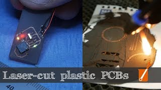
Making PCBs the RepRap way!

Вставка
- Опубліковано 29 вер 2024
- The first 500 people to click the link will get 2 months of Skillshare for free skl.sh/tomsanl...
RepRap 3D printers are built to replicate themselves as much as possible - and that includes fabricating their own electronics! Today we check out a way of producing PCBs that you can do on any 3D printer with a pen and a handful of 3D printed parts.
Parts used:
Pen mount www.thingivers...
Staedtler Pens go.toms3d.org/S...
Etching solution go.toms3d.org/N...
Ender 3 -_- go.toms3d.org/E...
Product links are affiliate links - I may earn a commission on qualifying purchases (at no extra cost to you)
🎥 All my video gear toms3d.org/my-...
I use Epidemic Sound, sign up for a 30-day free trial here share.epidemics...
🎧 Check out the Meltzone Podcast (with CNC Kitchen)! / @themeltzone
👐 Enjoying the videos? Support my work on Patreon! / toms3dp


3:34 for a split second i thought Tom was pouring superglue on the bearings hahah
Oh, it wasn't only me. :-)
Thought the same
It can help to reduce the strain on the moving parts...
Me to
superglue IS the best lube just add a pinch of unicorn fart and mix vigorously! I read it on the internet, it simply has to be true!
Halfway between both, if i am going to make a pcb (which i very rarely do when i can have a two layer made so quick and cheap) i spray paint the pcb and then throw it under the laser and have it cut the negatives for the traces exactly as you have.
I use a co2 but i think it would work just fine with a diode laser on a 3d printer. There are some inherent hazards related to that radiation which you'll have to decide how you manage but it has been the fastest and easiest method of diying it i have found.
Outstanding video, your content gives me tons of motivation, thank you.
I mostly use the iron-on method but I've been wanting to give laser a try.
@@chaos.corner I started with the iron on method and i think that worked well (assuming you calibrated your printer) but i found it took me a long time start to finish.
It's still pretty tedious to make a two sided board and you still have to be careful drilling regardless of which method you choose so it isn't perfect either.
@@giliant True. I mostly work one-sided which can take a little juggling and a few jumper wires but works pretty well. I have been moving to SMT though and that makes things a little trickier since through-hole stuff tends to give you freebies. My printer hasn't required any calibration fortunately.
This was neat to watch and very much reminded me of my electronics class in high school! We didn't use a pen, we applied traces via a sticky-backed material. Plus, our solution had an aquarium heater to keep it warm, heh.
I've heard of the ancient technology of sticky-backed traces, but have never had the honor to witness it myself.
@@MadeWithLayers Can you name some sites to download the example pcb design files. I'm a Mech Engineer and need it in dxf or dwg format
A friend of mine who was making custom audio systems back in the university. He was using a laser printer and glossy paper. Print out the PCB layout with the printer on the paper and then using an iron transfer the layout to the copper sheet. After a few seconds in eching solution he got the PCB. I have seen this method with my own eyes. Litteraly 5 mins and you have a PCB without the holes.
I have no experience making pcbs, but I was kind of thinking that pens would not work. What you really need is something like nail polish.
Idea for how to apply ink or nail polish or whatever very fast: make a stamp using a 3D printer. I have a little bit of experience with this, and what I will say is that a "hard" material like PLA does not apply ink to paper very well, because the paper and the bottom of the stamp do not fully come into contact unless you can deform one or the other. PLA works ok, but what you probably want is TPU (haven't tried TPU myself yet, but I intend to do that someday...). I'm guessing the same would be even more true for applying something to a pcb blank, since it's harder than paper, which means that you are really counting on the stamp to deform a little bit.
Sharpie permanent markers work for the etch resist. Have never heard of any other brand working for making printed circuit boards. Good video, Tom!
I second this
Interesting attempt, but getting the pattern right is only half the problem. Drilling holes and routing mount points is the next issue, and then making double sided boards which are increasingly required for anything other than widgets. Very hard to beat the Oshpark or pcbway offerings for this especially with their accelerated processing times for prototypes.
But, if you were to make such a system yourself, this is my wishlist:
1. Pattern drilling for all vias, mounting pads, and routed mount points. Has to be done BEFORE copper patterning.
2. Plate through holes for double sided processing.
3. Coat with resist and then laser expose for super precision, registering both sides for double sided.
4. Regular etch.
So, we need a milling/drilling capability, and laser resist expose.
OR - predrill and then 3D print a conductive material directly onto non-clad FR4.
As stated, these are all more difficult than the Oshpark options, but I appreciate the attempt.
Vias are the bane of all homebew PCBs I think.
I know the video is all about using the the 3D printer but the method where you print the PCB on a laser printer then transfer the paper print to the board with an iron, then etch is much faster, more accurate and a lot easier.
Great video - given the developments of FUSION 360, you should remake a printboard designed in Fusion 360, and using interphase to Creality Ender 3 in Fusion.
Ordered some CCL anti etching pens from ebay (also available from ali). Working well, but I do have some issues with larger areas. Still testing though.
i tried with a sharpie and it worked reall well, of coarse by hand though.
Use heated bed to dry out ink
I really liked using the 3d printer to heat and slosh the fluid, Very good idea. will you cover any other ways like painting the PCB and then using a laser to burn it away or toner transfer sheets or is this going beyond the 3d printing area you so expertly cover ? I brought a cheap XY vice that can be mounted to a pillar drill and tried that to drill the holes, it took a bit of practice, but it worked well enough to make a few boards.
The toner way is the way for DIY. ( prin on normal paper, press it with a iron, dump with acentone and alcohol solution and gently rub the paper away)
But, if you are willing to wait... china...
It’s not in the description; Where did you buy the PCB blanks?
I have a simple question - did you try to use a 3d print filament instead of a marker to draw paths?
Etching solution? timing? PCB copper thickness? anything useful? :/
Try Edding permanent marker
Someone's been watching This Old Tony.
yepp, i tought the same
Bit late but hey,
in the years when i wasn't alive (before 2000), people often used "iron" method of doing this. Basically, they had printed layout on paper with laser printer, then they put paper onto the copper, heated everything and the ink would melt, stick onto copper and bake onto it. Afterwards, they just etched it.
I tried this method many times when i was younger and it worked well. But later in school, we had to use a drawing method, which i got really used to, and here are some tricks:
- About the pen. You can actually buy specialised pens for PCBs, they aren't that expensive (i got mine with 0,2mm tip for like 2€), they work the best. Also i've heard the sharpies works good.
- Slow that thing down. While its drawing, it actually leaves a trace of LIQUID behind, and if its too fast, it draws that liquid with the tip, leaving indent in the liquid in the middle (the marks at the last PCB). When slow enough, the liquid will dry before that could happen, and it will be more thick (in Z axis..) thus more etcher-resistant, also it won't leave any marks.
- You can actually repair some traces/spots that has been broken whiel drawing by using very fine brush and acetone and/or sharpie again. Just underlight that PCB and you'll nicely see, where there's less ink, and just add some more. BUT, dab it, not draw. By dabbing, a literal drop of ink will disperse onto the surface, and there is a big chance of scratching off existing ink while drawing. So, dab.
- After everything is done and you like what is drawn, before etching, put the PCB in oven or heat it with a heatgun a bit. The ink will bake onto the copper and will resist etcher a lot more.
- Also i don't know what etching solution you used, but use ferric chloride. It isn't as aggresive to the ink as others and does a bit better job imo.
we still use iron btw
@@dhupee Yep, Iron with a laser toner printer is so faster, more precise and cheaper.
@@alexandrevaliquette1941 if you have laminator it's better
Much faster for me to print with a laser onto magazine paper, iron that to a board, then "rinse" away the magazine paper. The reason magazine paper works so well is because of how thin it is. Once the laser image has been ironed on (the iron remelts the toner, which then sticks to the copper), you just soak the paper for a bit in warm water, and it just breaks down and disappears.
But this IS cool.
Meh, laser prints are trash for masking, can never get them dark enough for smd traces... or any traces really, just cussing and filling the missing bits with a sharpie like a pleb, and if you're at it, just do it with a sharpie and a ruler from the get go. Or, you know, just get some photoresist film and do it like a normal person.
Edit: Regarding the etching solution, from the ease of use and availability, i prefer the H2O2/HCl solution - I mean, you can get peroxide and hydrochloric acid drain cleaner in any hardware store in any country. Also it's easier to work with, you can see the etching happening
3:11 ahhh... the good old TOT method. I never got it to work
Yeah, that's an excellent effect. ToT is ahead of his time.
Yep, you have to watch the "Clickspring Time Travel" vid!!
@@OzFaxFlyer I did back then. Also the wintergatan one and french guy cooking... Great minds and stuff ..
Ok.. There /has/ to be a HowTo video going around on just what the trick is! Many have tried. Only some seem to get it to work.
Maybe it's shared at one of the youtube creator meetups..
I'm going to stick to the hacksaw or grinder for now..
@@ElectraFlarefire I got it working on spaghetti. but nothing harder than that. at least not in 3 parts. I wish there was an open source wiki for that
This video is not sponsored by jlcbcp
Should it be?
Toner transfer is still my go to when i need a modestly complex prototype in a few hours
This is the kind of video jlcbcp needed.
Wondering about printing plastic onto the copper then acid etching
That's quite a sound idea. Especially with a smaller nozzle.
I was thinking the same thing. But it should stick really, really well then with resistive plastics and after the etching you should be able to remove the plastic without taking the copper off on the small traces...
I was thinking the same thing...
As someone who works with metal, its really tough to find an adhesive that bonds (reliably) with copper, I wanna say its pretty unlikely that it would bond well. But that was also my initial thought when I saw the title. Probably worth trying with different types of plastics.
So far PLA and PETG don't wanna stick. I'ma try other plastics
Tom, you brilliant man, I've worked in labs with heated agitator baths for years and I have never once thought to use my 3d printer for this purpose. My life has changed.
Yeah. I love how he just casually places the etching tub on the build plate that's already oscillating, without calling attention to it. Like, "oh, yeah, doesn't everybody do it like this?"
I love the 3dp as pcb agitator :)
Jup! Very clever! Why not?? It has a heatbed included for the acid solution... very very clever!!! 👍👍👍
@@Saartekk
Heatbed is not the best idea.
You have a large flat area, the liquid surface is losing a lot of heat through evaporation.
The simpler method is, use a zip-lock bag. My favorite is using FeCL3 etching, but it works the same idea using other chemicals too. I put a ball of roughly 2cm of FeCl3 in the zip-lock bag, pour in hot water, FeCl3 quickly dissolve. Then insert the PCB. Seal the ziplock. Put the bag flat down on a plate. The agitation is done by simply tilting the plate +10 degrees then -10 degrees.
Much better to laser jet print pcb artwork onto cheap photo paper then iron on to clad board never fails good results with good high resolution
My dad used this method, worked quite well. He used a modified laminator instead of an iron.
never got a stable results. always was some inconsistency in that method. either overheat or underheat, overpressed or underpressed, not enough time, too much time, not enough paper between iron and pcb, or too much paper. also highly depends on an iron you use. ugh.
just too much variables to control.
It's so much better, and in my opinion actually easier to print on a transparency, and use a UV lamp to expose it then, develop and etch. And you can do pretty much the same process to put on a UV solder mask.
Did it this way in school about 15 years ago. Worked a charm.
I think much cleaner method is using etch resistant paint and 2.5-5W laser to burn out pain and than etch.. plenty of videos on UA-cam and laser is much more precise than pen can and can be easyli attached to 3dprinter and enhance G code as well.. and it's just much cooler to use laser than pen :)
Yeah, but then you're using a friggin laser.
Thomas Sanladerer and the problem with that is .... what? That’s what they make laser goggles for!
Careful, copper is really good at reflecting the beam back.
A sharpie would do the job
The part made to hold the pen seems like it's a little bit over-engineered. Maybe one could design something with a little springy bit of PLA in one part. I thought of this after watching the Veritasium video on compliant mechanisms
Ferric chloride will attack the ink less than the acid you used I suspect.
I can use almost any permanent marker with ferric chloride
I was thinking he was gonna use that instead of the stuff he used
That works for sure. My father was repairing incomplete photolithography images that way back in the 80s...
I made PCBs with permanent markers (aka "laundry markers") with ferric chloride in the '70s. I wasn't the first.
The Fabercaster might work better with "ferric chloride
" ? The method presented by Heliox, is quite nice and in the RepRap way of re-using existing systems/component (and might be easier to pull off).
I also think it would be better to do it with ferric chloride :)
I use ferric chloride and when I see people use this other method on UA-cam, it just looks like a lot of faffing.
Yes, I built a pen plotter to make PCBs several years ago, and using a Lumocolor 319 S-9 with ferric chloride worked very well. Those pens are a little finer, at a 0.4mm tip.
I would love to see a variation where you attach a laser pointer to the 3D printer and use it to expose a photo etch PCB. The laser could be turned on and off using the fan control. Use your same program for generating the G-code and search and replace the Z changes with fan control commands.
Standard Sharpie permanent markers are typically used for masking PCBs. They're inexpensive, have lots of tip types, and the ink holds during etching.
I've never had any luck with Sharpie markers as etch resist. :(
@@Dosbomber My personal prototyping favorite was rub-on decals they used to sell at Radio Shack (yes, I am dating myself). You can still get these, but you really have to search for them.
I've never had ANY luck with any form of "permanent" marker on PCBs, and that's over 20 years worth of making PCB's using various different methods. The only pen that reliably sticks to the PCB and survives etching was the old Dalo 33 pen, which is no longer manufactured, and drew lines about 3mm thick so would be useless for any modern PCB.
Baking the ink in a stove for a while should have helped to cure it and make it more durable. Also, the etchant that you have used is cute, but it causes heavy cavitation which tends to remove even some harder resists. Ferric chloride is not pretty, but it does a much more delicate job. Really nice idea with the heated etching bath. Looking forward for the second video in the series ;)
And ferric chloride is simple/easy to make at home, so bonus points there.
@@LightGameFrameworks I never tried preparing ferric chloride at home. Would you like to share a recipe?
@@svofski there's tons of ferric chloride solutions out there. I personally use it because how hard other acid is to find out here and it works really well
I've been using laser diode to burn away the paint from spray painted copper clad boards, then etching as in the video. Super fine resolution and less problems with coverage. I believe there's a thread on German reprap forums about this method.
I use this method, too. Beautiful boards!
Mind sharing the type of the Laser Diode and what kind of optics you use with us? And what is the smallest size you can focus your laser dot (minimal isolation distance).
I'm using a BDR-209 diode at ~700mW power (400mA) with a three element collimating lens. I've recently bought a single element lens for supposedly better power transmission, and I might rise the drive current a bit for more power... All of this because burning away the paint still leaves me with a bit of residue that I have to scrub off before etching. Not sure if that's the lack of power or if my paint is not ideal. As for the spot size - I currently have it set as 0.05mm in my software. Can't remember how I arrived at this number honestly, but judging by the required overlap between passes, it's definitely 450nm lasers, just be mindful of power density.
Remember kids, always super glue your bearings for superior performance.
Edit: yeah I know
If the bearing doesn't slide freely you didn't use enough superglue.
For a moment there it looked like you were putting super glue inside of the bearings.
when I was young I used the Edding permanent marker and it worked really well also the staedler works well but you should check always the traces before put the PCB on the solution. I remember how I had to re-do the layout tons of times with my marker and ruler.
If complicated, when I ended that project my teacher told me that I could use a laser printer, and an iron to get the same result, but always checking the traces.
You can drill some registration holes to align the top and bottom layers for a proper dual layer construction.
@@-______-______- You can 3d print the alignment pins on the bed (with a larger base) and there you have it. Also you can 3dprint better pcb alignment and again, do not remove it from the bed until you are done with it.
I saw a film made by Tektronix in the 1960s, showing how they made their PCBs at the time. They used a photosensitive emulsion rather than plotting directly onto the copper, but they also did something else that may be helpful. Because they were making double-sided boards with plated through-holes, they first drilled all of the holes that needed plating, the holes had to be drilled before etching the copper. They also used plated through holes, which means that they couldn't just etch the copper directly, since that would etch away the plating they just put in the holes.
What they did was us a negative resist, that is, it covered the areas they wanted to remove, rather than the areas they wanted to keep copper on. Then they used a plating solution that very quickly plates a thin coating of tin on all exposed copper. Then they used an etchant that removes copper but not tin. I think they were using ferric chloride; I don't know how it would work with the copper chloride Thomas is using here (i.e., the DIY etchant made using hydrchloric acid and hydrogen peroxide).
In their case, the big advantage of this negative process was that the plated holes weren't affected by the etchant, but in the case of using resist ink as an etch resist, the advantage would be that the ink doesn't have to stand up to long exposure to the etchant.
As an added benefit, after you etch, the copper is already tin plated, which is a much better surface to solder to than is copper, and doesn't corrode as easily.
I should add, the tin plating solution is readily available and relatively cheap. I bought a 125 ml (4 oz.) bottle sufficient for making quite a few PCBs for about $20 on Amazon, but the price per ml goes way down if you buy larger quantities. It was called "Liquid Tin", made by MG Chemicals. The board only needs to be immersed for 3-5 minutes to get a good plating, and can be reused.
It’s great to show what you’ve learned even when things don’t work out, but the title of this video(“Making PCBs the RepRap way!’) is pretty misleading. Apparently, if you want to make PCBs, the RepRap way is to make three attempts at the resist method and then send your design out to a PCB fab company. How about changing the title to “PCBs with a RepRap: lessons in abject failure”? So: good video, but needs an honest title.
"You can't really drill holes with a 3d printer"
Really should watch this, where they mill and drill on the same 3d printer:
Simple DIY PCB with a 3D Printer - Tech2C
Yeah, He literally just did everything you would have to do other than attach the drill motor to his printer.
Who?
@@chaos.corner 3D printers are just not rigid enough so fixing that is somewhat involved. And yes every CNC router made by the 3D printer crowd that I've seen is a farging joke so far too.
@@1pcfred Well, we're talking of hobby level stuff where you'd probably be using a drill press by eye otherwise. Heck, I've wrapped some tape around a drill bit and twisted it with my bare fingers before. In that realm, a consumer level 3D printer would be perfectly adequate.
@@chaos.corner material does not care if you are an amateur or a pro. It is going to act the same way in either case. A machine that lacks rigidity is going to perform poorly regardless. Machine tools are not made out of tons of iron because manufacturers are just trying to get rid of the stuff. They're made that way because that's what works.
Why not just printing a 0.2 mm layer of ABS or TPU on it?
abs? abs does not stick to anything cold, and barely to anything heated
the marker soaks in to the metal slightly, plastic is to thick and also will not stick.
You do a good job on creating some original maker-oriented content that shows us that just tinkering around is often what teaches us the most. The "Play more work less" method :-)
I love your Videos ... but to store toxic fluids in a drinking bottle is a bad idea ... showing this in a video is irresponsible. I dont want to hate, but i think you have many viewers and some of them (IMHO) are young Makers. Please give them some safety advice, like wearing safety glases while working with this fluids.
"With great power, comes great responsibility" even with great youtube range. keep on making such nice tests, greetings from Berlin
Also worth mentioning some things like it's hard to dispose off and you can't pour it down a drain, etc.
Fc can be mixed with baking soda in a large bucket with water and poured down a drain. most drain cleaner is more aggressive city's add copper sulfate to drains to kill plant roots so i disagree on this also you can use the stuff for a long time i have about a gallon of it and it's about 2 years old still works. But agree about using a drinking bottle at the very least buy some crazy spray paint and paint the bottle. But think using a 405nm laser with pre coated pcb's can get you 0402 grade boards
Also, that bottle is very poorly-marked. I won't lie, I have stored chemicals in water bottles, but at the very least place some masking tape on the bottle and mark on that so that it's easier to read, since it's very clear that his sharpie label on the bottle is already smudged and almost unreadable.
All those soldering points should have etched hole in the middle of it. That small cavity on the copper helps to hold your drill bit at the center until the drill binds to the board. Hand-drilling these boards is really easy when the starting dents are already there. It also helps to see where ever you should make the holes.
I drilled hundreds of boards with centre marks in a plain ol' drill press in my younger years. We drill a stack of 3 at a time.
I would like to try marking out blue and a scribe in a similar isolation routing setup, I've got the blue and the scribe but no cnc /3D printer. I do have some stepper motors so it's not totally out of the question..
Just don't look to the 3D printing community when it comes to hooking stepper motors up. They don't have a clue how to do it right. the drives they use can't even push 2 Watts of power. It's pathetic.
shouldn't it be possible to use a DLP/LCD printer like the Anycubic Photon to create PCBs using photosensitive coated PCB stock? It should take only minutes to create the traces and also provide more than enough resolution. Did anyone try this?
That's a cool idea!!
I keep seeing comments saying photosensitive, the etch-resist is not photosensitive, its UV sensitive so it reacts to sunlight and some house lights but it only is reacting to the UV spectrum.
Yes that's how it's done in industry sometimes.
Try use blue laser diode for make pcb (1-3W)
You can use photo-etch boards, where you design your circuit, print it out onto acetate, & then lay the acetate design onto the board & burn the circuit onto the board then etch it with the acid.
Ferric Chloride would be better controlled than Nitric or whatever you were using. Doesn't look as good on video of course...
Seems like using a SLA printer LCD screen to project the PCB artwork on to light sensitive photo etch boards would be faster and better. Has any one tried it ?
Interesting idea. I guess you could also use any old LCD with the back pulled off and UV LEDs like that guy who made the mini SLA printer did.
I assume you would get a lot of light bleed on that method, also you would have to use a UV backlit LCD and that doesn't exist so yeah
Yes as long as you have a way to flip the art work and make a negative from the positive so that the traces and pads get exposed. Should work and be fast.
I thought all the SLA printers used a UV back light. And they do not have a bleed problem making the prints that are so incredible, so the PCB should be doable.
@@Robothut I have some spare LCDs and a UV spotlight. I'm tempted to give this a go.
I always just use plastic as a photoresist, some of the flexible filaments work quite nicely (dunno if it's polypropylene or TP urethane). By the way, fun fact: if you're drawing a pcb layout by hand, you can use a normal sharpie :)
I would like to see an attempt printing the traces with PLA on the copper clad, then trying to etch. Follow up by pealing the PLA off.
Post etch, it might pull the traces up - the glue that holds the copper on the phenolic board isn't horribly strong. Sanding the PLA away, however, might work.
@@jeffpotts6187
PCB are FR4/G10 not phenolic.
Modern Copper Clad is usually very tight.
Question is only how well the PLA sticks,
and if it resists the acid.
I use "phenolic" as a catch-all term when I don't want to look up specifics about what the copper is hosted on.
Secondly, I think you might be OK with Ferric Chloride, but with the other etchants people use I think it would eat away at the plastic. Ferric Chloride is considered caustic, but the others stuff generally IS caustic. With those, I think PLA would break down during etching. ABS and/or PETG, maybe not - but I wouldn't bet on it. I'm not a chemist.
That being said, it's less hassle to use a plain old Sharpie.
@@jeffpotts6187I see, you are not a chemist, you use catch all terms, and yet you know PLA won't work. Ok.
Toner transfer just seems way more reliable for diy pcb's? much more accessible than a cnc?
Toner transfer works for small pcbs. For big ones, things start to expand. I’ve made large pcbs with toner transfer and they ended up distorted and the wrong size from the transfer paper getting stretched.
@@skynet3d Fair, but for the size of the pcb Tom was making it just seemed like plotting it out with a 3d printer was needlessly complicating the process. For large pcb's I don't really see why you would choose a method like this over ordering through a pcb service though.
@@justintaylor2679 I wasn't implying it didn't work for what he was doing. I was just leaving the observation as advice for anyone coming across your comment. For large single side PCBs, if you already have a CNC or other way to make it yourself, especially if you're just making a one-off, it makes a lot of sense to do it yourself. Costs are not even comparable.
Awesome video. Love seeing people use modern technology such as 3D printers and utilizing them to make homebrew custom PCBs. This is what I call ingenuitive innovational progress! I'd like to take these concepts a step farther and see what we can come up with where graphene is the printable substance...
The old school method seems like it would work with fewer steps here... Instead of using your drawing to render the gcode for the pen, why not just print out the circuitboard drawing on a laser printer, and then iron the drawing onto the copper itself. Ironing the printed drawing causes the plastic from the laser printed process to adhere to the copper, which does the same as your pen.
because then you're not using your 3d printer to its maximum potential :) but yes, laser printer, toner, and iron are easier for the diy.
because you cant reprap self build a laser printer.
Wow, this is even more effort for less reward than UV lithography etching
Yeah, I tried both pen and cnc 15 years ago. Both were useless. Apparently nothing has changed. Except now you can get your pcb from China for almost nothing
You should explore if you could use the same process (hot end mounted pen) for something like calligraphy (think writing out wedding invitations or signing your name on a thank you card). It would be great to see the process you find from scanning a signature to creating an STL file to creating the GCODE etc. Cool video!
The question I always wanted to ask: why not print PLA on top of the PCB? No extra tools needed to attach. The only problem could be adhesion, which could be solved by soluble agents.
Nice try, but i'll stick to my laser printed transparencies and UV box thanks.
Yeah this is how I've been making my PCBs for a couple of years now. Drilling the holes is still a pain in the arse, though, even though I use SMD components as much as possible (including SMD 0.1" header strips). I've been using a Dremel in a Dremel WorkStation thus far (which I just discovered Mr Carlson uses as well), but my god it's tedious and I really struggle to align the holes well :/ And milling the outline of the board (eg if you want it a certain shape) is also really inaccurate :(
I've been considering getting one of those 3018 Pro CNC "engravers" - and ONLY using it for the drilling and edge cuts - but now I'm wondering if we really can't mount a Dremel (especially the small handheld end of the flexible extension rod thing) to a 3D printer's X-carriage and use that... 🤔 I would have thought that the Z-axis would at least be strong & stiff enough to drill the holes (I'm thinking about an i3-style machine here), and as it's only the up/down motion that has any force on it, I'd imagine it wouldn't really matter that the X & Y axes are weaker and less stiff. Using a 3D printer to mill the outline (and any slots) would be much more tricky, though :/ Maybe with a high enough tool RPM and a slow X/Y feed rate it might work ok?
My ears are ringing just at the thought of being anywhere close to that thing while it mills the edge, though 🙀
I'm definitely wondering if I can adopt Tom's etchant heating & agitating technique! 😹 Main issue is that my printer is up in my bedroom, 2 floors above the kitchen where my PCB equipment is stored, and I really don't fancy having all those chemicals up in a carpeted bedroom o.o I do have a couple of spare heated beds, though (they're crappy and very not-flat, but they still heat up fine!) so maybe I can just hook up something with one of those, Marlin, an Arduino and a decent MOSFET (maybe just one of those external heated bed MOSFET boards for simplicity). And since I use the Seno GS system, my ferric chloride is always inside a sealed plastic "bag", so I could probably just sit the Seno GS bag directly on the heated bed 🤔 Maybe a single-axis platform movement system wouldn't be too complicated to rig up, too 🤔
Thomas,
Could an FDM 3D printer with a small enough nozzle directly deposit a plastic etching mask layer to a copper-clad board? Would any common filament materials like PLA, ABS or PETG even survive submersion in FeCl during etching? You'd have to be careful removing the filament layer when you're done to avoid lifting copper pads, but luckily these plastics have a much lower melting temperature than copper or especially fiberglass, likely meaning you could burn it off without too much work. Maybe there is a second chemical bath that could dissolve only the plastic, leaving the copper and FR4.
I'd really love to see this tried out in the future!
Years ago, I used to draw the PCB graphics by hand with nail polish before any pens, home cnc's etc. were even conceived. Worked like a charm, do the results were only as good as your artistic skills.
You've been watch "This Old Tony".
Just use a paper-printer and print in mirror. then iron it on the pcb, put in water to remove paper layer.
Then put in etching solution and wait. very precise, perfect result.
You can see the pen running out of ink because half is sort-of ok, and the other half is poor. Also solvent based ink tends to dissolve it's own lines if it touches deposited ink. Maybe a new pen and a smaller PCB and it might work. I put a 0.4mm holed pad on each THT pad as a guide to locate the drill bit accurately, etch and tin the PCB, and the step left in the centre of the pad is enough to guide the drill when I drill them.
Instead of using a pen, physically print the circuit with TPU - works well.
how consistent is printing TPU onto copper?
I love how 3D printers can do so many non 3D printer-y stuff
Nipuna Gunarathne like removing tomato’s from a salad
Who wants them in his salad tomato gets stabbed
I suggest when plotting to heat up the bed to aid in the ink drying. Also, I've had pretty good success with sharpies doing touch up on the laser printer/iron process. Not sure how hard it is to get a sharpie where you are.
I mean no disrespect, but this seems like an awful lot of work for a single-sided pcb, and the results were frankly sub-par. I use a modified laminator, and can print the pattern, apply it to the blank, etch in a HCl/H2O2 solution, tin, and drill a double-sided pcb in less than an hour. It is a shield for an Arduino Mega, and uses every one of it's pins, so it's not a simple pcb; it has about 300 holes to drill ....
Wouldn't a small Dremel like tool attached to the extrusion head work for drilling PCB's? Downwards pressure should be in the same ballpark as pressing down a Sharpie. And if anything's gonna break, surely those sub 1mm drill bits are the weakest link, I'd recon. The hard part would be preventing vibrations. Perhaps a small high rpm DC motor, like you'd find in RC cars, could work.
Well, I tried the same a few months ago with better results.
First, those stainless steel guides are too much for this, you should use a smaller diameter ones to reduce the weight. I used 3mm diameter rods with lm3uu.
Second, try to reduce the head movement before attaching the pen mechanism. I don't recommend use two side tape to keep it in place. Instead you can design a piece that attach perfectly to the head with some screws and nuts.
Third, always use black permanent marker and, as you said, check the ink flow before start. I recommend use alcohol to get the tip wet and roll in your hands vertically with the tip pointing down.
Fourth, reduce the pen up distance, it's a waste of time. 3mm will be enough.
Fifth, I had better results at faster speeds (not too fast but faster han in the video). The problem is if the pen keeps touching the copper will make a tiny blob of ink that will increase the trace width.
Sixth, the best way I found to make a PCB in the correct place is moving the head it an interface (like Repetier one) to a corner of the copper board, touching it enough to draw and set that point as the origin. In the gcode file you must place the PCB drawing with a corner in the origin and of course remove homing commands.
Seventh, if after the draw is complete you see the copper through the ink, re-draw it over the previous layer. Make sure the ink of the previous one is dry. Don't move the board from the bed, just execute the same file and it will draw exactly the same in the same spot. Maybe you will need to adjust the z position a bit to reduce the pressure of the tip over the board.
Last, place the PCB with the copper side facing down when etching (not touching the bottom of course) or keep facing up but move the board like shaking. Will be a lot faster.
Good luck!
When are we (you and the community) going to start building the ideal 3D printer?
Probably never as there isn't really such a thing, everyone has their own use cases and specific requirements.
The edding 140 S works perfectly.
I've been making my circuit boards this way for about 30 years, except that I bought a pen plotter specifically for it. This procedure gives better results than you think. Running a conductor track under an SMD resistor of size 0805 is not a problem.
If you are interested in how I produce printed circuit boards with my plotter, you are welcome to watch the video “Die Leiterplatte” . Video link: ua-cam.com/video/5d-9P_2lBAY/v-deo.html This video can also be found in the Kinetische Kunst / Werkstatt playlist located on the Kinetische Objekte UA-cam channel.
Just use laser printer or technique or UV films and negatives.
Oh and a marker won't stop the solder at all...
they all have great ideas but it's NEVER taking less time than usig my printer and iron. personally i'm thinking of getting a small flocking heat transfer press, i'm looking for speed and efficiency not fancy technical procedures.
As usual, the solution comes from China - don't use an expensive STAEDTLER marker. What you really need here (and I can guarantee this WILL work) is.. A cheap TOYO permanent paint marker. How do I know this will work? Well, quite simply, cause I make PCBs sometimes. I use the old and trusty laser printer method (there's also the photo-resistive coating method which is more professional, but I don't use it since the laser printer method is good enough for my simple projects). whenever the toner doesn't transfer, I use a TOYO marker to fix it. Works every time. Try it. EDIT: Before you use a TOYO marker you need to prime it (press it until the paint start flowing) and if you print on heated PCB it will dry instantly. I think heated bed at 60-70 degrees should do it. Funny thinking a cheap chinese paint marker will out perform an expensive steadtler marker on this.. Only that's exactly what will happen. Happy PCB plotting!
To etch FAST (
All these make pcb on 3d printer are all about using permanent marker in special attachment.
But why can't anyone print the mask using one layer of ABS/PLA/etc with 0.2mm nozzle?
This makes more sense for 3d print community.
Probably, Wood's alloy can come handy, as table can be heated above melting point(70C).
Thomas.
Thank You for this video.
Probably If You have had cleaned and degreased PCB carefully before plotting, result was much better.
Good solution for cleaning is Cif - cleaning crema with microcristals. It removes well corrosion from cooper as well as grease.
You need to clean untill water covers perfectlu whole surface of the cooper.
Then ink should cover traces it perfectly and etching solution proof.
From my experience the best etching solution is B327 - Na2S2O8. It is not so agressive as acids, and not so dirty as FeCl3, but could ignite flamable materials.
This might be a silly idea, but couldn't we just print PLA etc directly onto the copper, the peel it off once etched?
The black traces floating off were kind of artistic. Farewell RAMPS!
I bought a $60 Laser Printer and a $5 magazine to print my PCB diagrams onto and a $6 bottle of nail polish remover to transfer the toner (perfectly) to my board. $10 gallon of Muriatic acid (which should last me nearly forever 😂) from the hardware store and boom, perfect PCBs. The acid eats the copper so quickly that the toner (which is melted plastic so it doesn't corrode anyways) has zero problems with trace definition. Even with traces as small as .254 mm wide.
Very bold Tom! Not only are you pouring liquid over a printer, but also hoping that the tub isn't super cheap and melt due to a hot spot! Also, thermal camera Android app? Where do I get this?!
First PCB's i made were done with laser printer transparencies and UV reactive coated boards. Theyre probably still floating around in some medical devices in a hospital somewhere. A photocopier also works really well for the transparencies. It means you can do double sided PCB's easily, up to A5 size, by creating a mirror of your files and folding along the centre line on an A4 transparency. Its not accurate enough for hairline tracks, but if you stick to fat boys then you're golden. Then just expose to UV light to develop.
So 30 min for nothing...nice!
builds a super rigid overengineered pen holder: Clues it on a wobbly fan :D
Damn, when will they introduce memes to youtube comment section
Would there happen to be a tutorial showing how to do the things you said to do in flatcam? By the way, I love your videos Thomas.
I would not do it this way. I would use transparent film to write on by the 3D printer. Then use IR lamp on Photo sensitive PCB. The result would be 100 times better. Its harder for it to fail then.
Hi there. New subscriber to the channel. Enjoying your work.
If you have access to a laser engraver / cutter there is a much more reliable method. 1st spray the entire board with a basic gloss car paint then convert your PCB mask design to a simple bitmap. Drop the prepared PCB into the laser and ENGRAVE away the paint to leave the copper to be etched bare. After a light wiping to get rid of any left over paint debris the boards can be etched to reveal the PCB. A quick wash in acetone removes the rest of the paint leaving the finished high quality PCB. I work in a school and use this method to batch produce 100 PCB's at a time and it is much more reliable and WAY cheaper than using photo-etch resist copper clad board and more accurate than a pen method. I almost never get any failed PCB's at a fraction of the cost AND time. With this method the drill holes can also be reliably etched into the pads making drilling much more accurate for students to do. I hope this is of use.
Heh, still with the Staedtler red pen as etch resist huh? You can get finer Staedtler pens too, you need the UltraFine instead of Fine, and Sharpies work as well - blue or black. They also come in UltraFine. I used to do this back in 2003-ish with a HP pen plotter with the Staedtler red pen mounted into a hollowed out plotter pen housing. It worked ok, but I only did it a few times. Toner transfer using magazine paper worked a lot better, and these days commercially produced PCBs are so cheap, why would you bother doing this at home? You get dual layer, plated holes, solder mask, and silkscreen for next to nothing these days. I'm sure it actually works out more expensive to do it at home than to ship it out to one of the fast pcb prototype services. Only real advantage to doing your own PCBs at home these days is you can make a PCB RIGHT NOW, as opposed to waiting a few days, if you have your process dialed in.
Thomas, don't give on 2D drawing PCB designs onto copper just yet. I bought a pen in Japan called a Uni Prockey Twin, made by Mitsubishi Pencil Co., part number PM-120T, that has a tip on each end, one fine and one two or three times thicker. Don't know the diameters but I do know that it worked fine as a repair pen for a PCB I made recently using the nail-polish-remover-toner-transfer method. I suggest you outline the drawing using the fine tip first, then fill in the voids with the fat tip. This could preserve resolution without making wave patterns in the voids. I don't know if there's enough ink in the pen for a decent sized PCB but it won't hurt to find out.
Hey, here's a crazy idea: Why not print the tracks in PLA or another plastic that the 3D printer can handle directly on the PCB? I mean, that's somewhat the whole idea with PCB Toner transfer... toner is a mixture of plastic and pigments that gets melted on paper (or a PCB in our case) providing a pretty nice etch resistant mask. I think it would be quite fiddly to get this working, and you'd need a very flat PCB surface to begin with... anyway... I think this would be an awesome idea for a video!
What about using the 3D printer to print a single layer of usual plastic (ABS or PLA, I think both should be resistant to iron chloride) directly in the PCB surface instead of the hot bed?? I know resolution may be not very good (the nozzle diameter, usually 0.4 mm) but probably the printed layer isolates better the acid than the marker layer, since it is much more thick. I may try it someday. You just need to recalibrate the zero of Z axis to be the surface of the PCB...
I'm just failing to see why one wouldn't just use the toner-transfer method with a laser printer, this looks about as reliable but far slower and requires you to build a pen plotter adapter for your printer. Even if you don't own a laser printer, it isn't too hard to find one at a print shop or local library, and then the only special required tools is an iron (or a modified laminator if you're more serious and willing to spend $20)
Edit: for anyone interested, the real trick is to go into printer settings, and at least for my Brother printer: 1) ensure toner saver isn't selected 2) Change resolution to highest setting 3) advanced->other options->improve output->de-select improve toner fixing 4)density adjustment->change to darkest 5)transfer to the PCB as quickly as possible, ideally have the pcb ready to transfer before you print
And although it's arguably more of a PITA, I've had much better success using ferric chloride than other etchants
Nice Video, but an PCB will cost less than the Pens used and you will get the PCB drilled, 2 Layers and higher Quality. In my Opinion it's not that usefull if you can wait some weeks to get the PCB manufactured. There are only few cases you want to etch it yourself. Next Point is you can't just flush most etching Chemicals in the Kitchen sink. Anyway, just for Fun it will be fine ;)
interesting attempts... but the results are a bit anticlimactic.
Sometimes it's about the process and not about the climax
@@MadeWithLayers we learn far more from our failures than successes
3:10 This old Tom... you shenanigan-fu is strong!
The other problem with this is that the center drill hole for the pads is filled in. That might not seem like a big deal, but when you can etch out the hole (even a portion etch), your drill bit will "Self-center" into the hole, making it much easier and accurate to drill
Normally: use scotch brite as fine as you can find , scuff up the board
then draw /iron on your laser printed schematic.
use STRONG etch if you use pen! it will go faster , and the pen might last just long enough to cover it all. (i think iron chloride? been a while for me)
then clean etc.
You might want to try without a elastic, the weight of the pen and carriage might be enough..
Check out Dirk Herrendoerfer direct ink to pcb plotter here on youtube.
This is just messing about for results that, even with a perfected process, will suck. Negative dry film etch resist (Dupont Riston or similar) and Bluray (405ish nm) laser pointer what I'd try if you insist on using a 3D printer to draw the artwork. Then ferric chloride to etch.