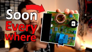
Mrf300, amp testing, amp boards made by Vk amp.
Вставка
- Опубліковано 8 січ 2025
- Update 15 March 2021
After looking at other designs,
knowing now that I have the wave form looking good on my board, the third order harmonic is still poor, the boards are just not able to get to there rated power figure , seeing how other designs are cleaner and making close to the devices rated power.
I have decided to scrap these boards, save the mrf300 ‘s and the other bits worth salvaging,
move the devices over to a proper designed and performing board.
Video to follow once it’s all sorted, In the mean time a mate is sending his board down , the same as the two I have and I will do a test with his board and see how it compares to mine.
As all 3 boards are different even though made by the same guy.
It was a expensive lesson, That lesson is buy from guys that have been doing it for a while, not the new kid on the block .
Update 13 March 2021,
Buyer beware I guess !
Here is the second place winner in the Nxp design a amp challenge,
Here he gets the same power out put and better efficiency
With far better harmonic suppression .
Why would you bother to put 4 device on a board?
You would be just better off combining two of these boards, be careful where you spend your money guys ,
it should not only look good, it should perform too.
• A 600W broadband HF/6m...
Or this video where than man makes 1200 watts
With four devices
• HF/6m linear amplifier...
As for my underperforming board,
With the help advice of a long serving RF tech in Aus
And another, a, ex B.A.I RF engineer,
I pulled the 4 ldmos device from the board and did a ohmic test
None had a gate to drain short and all could be turned on, none measured bellow many mega ohms, no faults on the ldmos could be found.
So,
Again under advice from trained qualified professionals,
We just fitted two, to one side and did a scan, then removed, and fitted the opposing pair and did a scan and then re fitted all 4 and did a further scan
After cleaning up balls of solder around critical caps, the same issue I found with the filter board along with a solder short under a relay.
Sloppy clean up by the amp builder?
The scans are better than the day before.
Yet still indicates a impedance and or phase mis match .
The fact I had to add a line transformer , ie a piece of coax to make the amp work in the first place and measuring the filters with the xtra line length ,
Showed the filter to amp board swr improvements
Also showing an improvement on the meter between the boards to the filter.
This indicates the amp board is not properly matched .
And why it loses so much power on 40 mtrs
The advice now,
Is to go thru the circuits after the drains ,
I now have a mock up board and the 9:1 and 1:1 transformers on the mock up board.
We are now seeing this impedance issue!
The 50nf dc blocking caps, add a additional capacitive reactance after the 9:1 these are playing havoc with the phase angle after the 9:1 transformer and plus there is additional positive reactance on the 1:1 balun that has not been compensated for.
This looks like the impedance Imbalance messing up the wave form.
Also there is 380pf difference between the right side and left side of the Dc blocking capacitors causing further imbalance.
So the R and D continues .
It is getting closer !
Why all this work?
Losing 320 watts on 40 mtrs is not acceptable .
Update, 12 may 2021,
Starting to look like the faulty filter board from
The vic AMP builder may have taken out a ldmos or two
And this may be causing the non lineararity issue with a device or two that may be no longer functioning on the board
The current protect board due to its early failure may not have been
Able to limit the current as it should Have?
The testing continues.
It was suggested by Tony and his RF engineer mate,
That the wave form issue on my scope was due to looking
Between the pa output and the filter.
This was messing up the pattern?
They inform me!
thanks Tony.
Only issue was , I had no filter connected at the time of that test?
but a pic only shows so much .
So here is a video, showing , 10 watts rtty carrier into the Pa board, 670 odd watts out from the amp board.
This is the wave pattern you see in this video .
Houston we have a problem!
The amp builder from Victoria will not accept he may have it wrong,
Even after he got it wrong with the low pass filter .
Later , after the video was made,
my mate, sends images of his amp board made by VK Amp in Victoria ,
And bugger me, we find that my two boards are not the same and both are different to
My mates board.
We are talking different values in the feed back circuits on all three boards, difference in attenuators and freq dependant attenuators,
All 3 boards are different .
How can I combine my two boards when there not the same?
All will become clear when my mates board arrives for testing in my amplifier .
Further video to follow .


