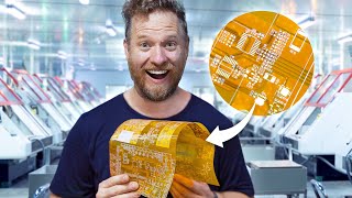
JLCPCB Factory - 2-layer PCB Manufacturing

Вставка
- Опубліковано 14 жов 2024
- $2 for 10 PCBs (2-layer, 48hours lead time): jlcpcb.com/e
The monthly production capacity is 200,000 sq.m. PCBs in JLCPCB factories, The video shows the whole manufacturing process of 2 layer PCB in JLCPCB Daya Bay Factory :
Step1 From File to Film
Step2 Material Cutting
Step 3 Drilling
Step 4 Copper Deposition
Step 5 Image the outer layers (dry film, exposure, developing)
Step 6 Pattern Plating
Step 7 Etching
Step 8 Automatic Optical Inspection(AOI)
Step 9 Solder mask
Step 10 Silkscreen
Step 11 Hot Air Solder Leveling(HASL)
Step 12 Profiling
Step 13 V-cut scoring
Step 14 Flying Probe Testing
Step 15 Packaging & Delivery
PCB Stencil Factory • How to create PCB in a...
The World's Greatest Electronics Market - Shenzhen, China • The World's Greatest E...
Facebook / kasyan-tv-139150916827430


Never in my life did I think I would learn how to design PCBs for my hobby arduino projects. Now I am designing boards and ordering in super low quantity, yet the pricing is almost too low to believe. It's just awesome. After watching this video I'm almost embarrassed that these people are working so hard, and somewhere in there is my little order of 10 PCBs for my home project. But without them, I would have never taken the leap. Cheers JLCPCB, for offering these services to hobbyists for such good prices.
Yeah its crazy, it opens up so many possibilities to create high quality projects 🤩
Just few days ago I ordered my first ever pcbs from jlcpcb :D Can't wait for them to arrive :)
First time order , the quality is amazing. It’s crazy how accurate these machines and people are for that low price. Very pro work
I just ordered my first simple PCB's last week are they are ready to ship. Great job guys and girls. You are the best.
Amazing. Even more so that they cater to small orders in such a highly automated factory environment.
I am very happy to see this factory, Thank you very much lady.
Cool video. I could listen to your voice all day.
I saw one person smiling, I hope he didn't get fired !
One question, who is the guy with the JLPCB black shirt?
Amazing process.
Great video.
wow... supercalifragilisticexpialidocious thanks...:)
This factory needs people to load and unload machines and robots.
Low skill labor, means more profit.
World-class operation.
And I think the bearded guy does all of that work! He's everywhere on this video! haha
He is Kasyan. The Chinese girl, is his girl friend who does his video narratives.
@@ufohunter3688 I am not that guy, I'm the guy who make projects and shot videos for my channels)
At what stage the pen gets in?
Excellent
Great vid 👍👍👍👍👍
who knows what is partial cutting? isn't the outline required to be closed? can I draw only a line instead of a rectangle?
VERY NICE.......!!!!!
Very cool. Thank you.
It does look like aging tech, zero health & safety, zero enviro, and dirt cheap labor. Still cool.
most of the plant is automated. Workers are wearing PPE. There are dust collection systems. I don't understand your complaint.
Nice video
Wow.
Hi
I need smartphone battery protection pcb
15:42 someone is making Arduinos
what a great company. They say dry film photoresist used in factory. its a bad way for producing pcbs with tracks below 12 mils. They should use positive photoresist method. Negative photoresist is not giving good quality. i can make 0.2 mils of tracks with positive photoresist.
It may be worse, but it is cheaper, especially when pumping out millions of boards every year
why do you have to show this ze alley in a black shirt you have to show are the employees working untested
6:35
Haha what the fuck