EEVblog

Вставка
- Опубліковано 24 вер 2024
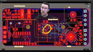
- Dave looks at some issues with fanning out tiny 0.4mm pitch BGA packages, via pad and hole size, tenting, breakouts, solder mask expansion etc.
And then compares it with an 1136 pin Xilinx Virtex 5 FPGA with 1mm pitch to show the difference in PCB process technologies needed.
FPGA Implementation Tutorial - EEVblog #193
• FPGA Implementation Tu...
Forum: www.eevblog.com...
EEVblog Main Web Site: www.eevblog.com
The 2nd EEVblog Channel: / eevblog2
Support the EEVblog through Patreon!
/ eevblog
Donate With Bitcoin & Other Crypto Currencies!
www.eevblog.co...
EEVblog Amazon Store (Dave gets a cut):
astore.amazon.c...
T-Shirts: teespring.com/s...
💗 Likecoin - Coins for Likes: likecoin.pro/@...


"This is not a particularly complicated board" Dave Jones 2017. Gold
Hey, Dave! Man, I can't even explain to my fellow viewers how valuable this video really is!!!! I just wish you had done it MUCH sooner :)
Trying to find some of this info for a hobbyist is damn near impossible. I'm a software guy by trade and have no formal education in hardware. It took me a couple of years to piece together enough information and thousands in re-spun boards to finally do a working design with a small-pitch large ball-count BGA chip.The fact that you did a video on this is going to help SO many people who don't know where to start.
Every FPGA manufacturer has recommended fanouts and even PCB stacks for individual packages/families. Its not like it is that hard to come by to this info on web.
Fanouts are about 1% of the board layout. I wasn't saying great job for showing a fanout. I was saying great job for the info in the video in general. Via sizes, via tenting, layers, bypass cap placement, and he even mentions IPC guidelines, which took me months to come across by accident on my own. If he broke this video down into a few more in-depth videos, it would be amazing for the hobbyist who wants to get into this kind of PCB design.
Unfortunately these examples are very outdated nowadays. Modern hi-speed buses like DDR3 have very strict requirements on how do you route them out - you can't just spread them around however you like. This makes using "default" dog-bone fanout (which even cheap tools like DipTrace can do nowadays BTW) near-impossible, and you have to craft it to make sure certain trace groups go to specific layers regardless of where they are on device - and more often than not you're quite limited in amount of pin-swapping you can do to aid layout.
Another factor which makes routing BGAs harder is the fact that you have to make do with as few layers as possible. I'm a hobbyist too, and making a first 4-layer board with Artix-7 device (256 ball 1.0 mm package) took me weeks of reading datasheets, appnotes and guides, as well as actual routing - I had to scrap routing and start over several times. The information is out there, but it's extremely hard to find. Currently I'm working on my first 6-layer board as I've managed to find a fab that claims it can do such board with CI and tight tolerances at reasonable cost, and this is a huuuge improvement as 6-layers add two more signal layers so making layout much simpler.
As for bypass caps - it's no longer enough to just put them under the central part of FPGA, as IO banks need their own local decoupling, and placing them near IO banks power/gnd pins can seriously hurt your ability to route out signals on the bottom layer. So much so that on one design I have opted to make the bottom layer my ground layer on a 4-layer board, instead of "conventional" sig-power-gnd-sig" stackup.
Oh, and last note - it's VERY important to understand that hi-speed controlled impedance traces need REFERENCE plane, not ground plane! Power plane will work just as well provided that signals actually use that power plane's voltage as IO voltage from that very supply rail (VERY VERY important note - if signals have same IO voltage level, but are actually coming from different power supply - it won't work as current loop will have to return current back into that remote power source). This understanding (as well as consequence from it - power plane needs to be as good and solid under/above traces as ground plane normally is) will help you to route things out on fewer layers - as a matter of fact, this is the only way to route 4-layer boards as well as 6-layer ones (as both typically have only 2 plane layers, and all signal layers reference to one of them). In general - whenever you route hi-speed traces, always think about how return current will reach the source, and do your very best to ensure this return leg is as short and as low resistance as you possibly can.
Good to see there are other hobbyists making their way into more advanced PCB design! I've been where you are now and it was very frustrating. And trying to get help from engineers that have done this type of layout before was useless. It's absolutely as much art as it is science to lay out this type of board. And people who know how to do this type of layout are not very keen to give out that information.
However, I hope you aren't saying that Dave's examples are outdated. This kind of info is never outdated. Not all chips use DDR3 and have high speed busses like USB3, etc. Some of us still play with chips like STM32's that need just the type of layout like Dave was showing above. His examples are still very relevant to anyone who is just getting started in this area.
Also, if you need any advice on the best PCB fab houses to get 6+ layers done with excellent tolerances without going broke, let me know. I've tried more than 10 fab houses and found that only a few could produce high-yield without costing thousands of dollars. Feel free to contact me for any other pointers on this stuff. I promise, I've been there.
Well the thing is - in many cases I wish I would have an option not to deal with DDR3 and go with DDR1 instead (as DDR1 is available in TSOP packages, unlike DDR2/3, which is 0.8 mm pitch BGA only), but Artix-7 devices are not even electrically compatible with them. Same deal with more-or-less modern CPUs and SoCs - DDR2/3 is pretty much a standard there. So - year, as soon as regular SDRAM speed is not enough for you and you're not willing to spend a fortune on big SRAM chips, you're pretty much stuck with DDR3 and all headaches it brings into design.
I would really like to hear about affordable fabs, but I'm not sure how to do that on YT, if you're on EEVBlog forum, please send a PM to user "asmi" (that's me). I would appreciate any experience you're willing to share.
Hands up. Video on pinswaps would be cool :)
Long ago I got fed up with the nuances of BGA fanout/layout (and my large number of wasted spins). These days I import a known-good reference layout and tweak it to meet my needs, sometimes even merging sections from multiple reference designs. The NRE savings are huge, which can provide the money needed to get more layers on the production board.
It doesn't *always* work out. Sometimes fewer PCB layers are mandatory, and much more work is needed. But that's when I contract the work out to a true expert, and still make savings on both schedule and NRE.
I've even done this on two hobby boards, where I traded writing some software for the BGA layout. We both win! I can write much better code much faster than I can do difficult BGA layouts.
I do have a favorite trick when I have to handle high-frequency controlled-impedance signal pairs: I can sometimes get away with hand-soldering some thin coax (RG-174 for signals
I am on the other end of this process (We make semiconductor devices) We generally expect everyone to do as you do, in fact if you insist on making your own layout our support guys will likely tell you to use a reference design.
Part of our process, way before even RTL is started we make preliminary PCB layouts to ensure the device actually can be used.
We do make a lot of effort in making sure we use a minimum number of layers, minimize vias etc avoid fine pitches etc on these reference designs.
Watching the PCB videos is what, to me, makes electronics feel the most simple and accessible. Please continue making more! :)
Just submitted my first two layer PCB to manufacturing yesterday.
Congratulations! 😎👍
Extremely informative on how dense boards are made. Thanks for the explanation and examples.
I really enjoy the PCB design topics. Not only because I like to use Altium as well, but a lot of your explanations carry on past the specific EDA software. I've been watching you since around episode #200 and you're the best man!
Thank you Dave, I really enjoy your PCB layout tutorials (especially Altium related), fun narration, great practical advice and you don’t assume we know everything like other tutorials do! More please (if you have the time). Dom
I will love every pcb video you made, LET'S FAN OUT
FAN OUT FANBOY!
"For those of us playing along at home" *Pulls up data sheet on second monitor to go along with video.
Nice!
And what's on third monitor?
Well 2 ultrawide costs much more, than 3 regular one IMO.
I dislike ultra big monitors, I find more smaller ones with one bigger main monitor works best, because the monitors create natural snapping points better. You can, for instance fullscreen a video player to a monitor. Just try and get a video player to "fullscreen" onto a part of a display... My main computer has 4 monitors hooked up, one big one, and three small 1280x1024 17" ones. And as a bonus, I've only spent like 20 euros total for all the secondary monitors buying them second hand.
1280X1024 is definitely the best resolution for datasheets and documents. Widescreen lacks the vertical resolution necessary for lots of things, unless you mount it 90° rotated. Finding 5:4 aspect LCDs is super easy, and as you mentioned, cheap. I picked up several 19" for $5 once.
I like the video. I have used my first BGA one year ago. Fortunately everything worked perfectly. But now I have moved to a equivalent LQFP version with less features, because the BGA made the PCB very very expensive. I fixing the missing features in software now with is pain in the ***. But it worth it.
Always great to see a practical pcb video. Thanks Dave!
+1 to pin swaping video
Definetly more PCB videos
Kristjan Orn Absolutely!
Many pcb manufacturers told us not to tent the vias, because chemicals can not be cleaned out of the holes properly and lead to corrosion. On the other hand, tenting reduces the risk of shorts. What we did is almost completely tent, but leave the holes open.
After watching a chunk of this I have all new respect for the undoubtedly challenging pinout on the Raspberry PI w!
*raises hand for another video on altium designer* Great tool that, too bad I can't afford it. I wish you had shown the footprint of the two devices next to each other, just for the effect.
Laser drilling and routing is actually getting quite affordable with newer production systems. Sometimes it's more economical to laser cut/drill than to go for the old mechanical solutions. An added advantage is that the high-end systems have multiple heads, meaning they can actually beat the older systems in board throughput on complex designs with thin FR-4 or flex. Many manufacturers simply massively overcharge for what they consider a non-standard process flow.
Hands up on learning more about pin swapping. Would be nice to learn more about that!
Very nice video! More PCB stuff is always appreciated.
33:30 lol ^^
That is really cool though. Instantly made my brain go click seeing that when it comes to how multilayer boards work. So you always drill completely through but only connect onto the required layers. Neat!
Expensive but easier package can compansate additional Pcb cost ! VERY VERY GREAT VIDEO. THE ÖNE OF BEST I HAVE EVER SEEN. THANKS A LOT SIR. I hope you will introduce my big high speed upcoming board next year.
You inspire me to try the more challenging. Thank you
nice work Dave
Love this video! Really helpful for learning the more advanced features of Altium. Would love if you touched a bit more on the pin swapping in another video and how it can be used for other packages as well and not just FPGA's (BGAs).
Love the PCB videos and would like to see more please
the 1136 pin part also shows another problem, with all those vias you can quickly end up with very little of the planes left under the part. Afaiu it is allowed to skip the annular ring on on unconnected layers, that will help a bit
Yes please, do more PCB stuff, love it! Great video
More advanced topics like this ! Thanks ! :)
Would love to see more PCB related stuff! Great video. Thanks for sharing!
Thanks Dave. More PCB design stuff please. I use AD at work so I am always wanting to learn more about it. Tricks and tip are also valuable :-)
I Only Just Checked To See If EEVBlog Had Uploaded A Video... And Then The Notification Popped Up :)
Spooky
I made an expansion board for my DE0-nano in Dip Trace a couple years ago and dreamed about such feature as pin swapping. Maybe it is time to try Altium. Thank you Dave for this video.
The poor AMD Threadripper enginners... Thats 4094 pins to route on the TR4 socket. Granted, many are power and ground, but thats still a clusterfuck of pins.
Luke Den Hartog they also get lots of layers on the pcb. Still takes forever though
IBM's latest mainframe PU design probably has even more pins than that considering they've gone fully parallel in the last two generations.
I tried to layout an LGA-2011. Just trying to get the various power planes to the pins they needed to go to drove me batshit crazy. You have to take into account current requirements, heat dissipation, etc. Needless to say, I did not finish that board.
The PCB guys that design motherboards are true masters of their craft. There are SO many rules and variables that have to be taken into account.
Silver award
This might be a dumb question but is there a reason why you couldn't just use the vias themselves as the pads you solder the BGA to?
It would be great to see a pin swapping video too!
pcb's should indeed be works of art!!!
Hey Dave,
Sure enough, I wanna see PCB design related stuff more! Very nice video indeed! Thanks!
Thank you Dave! This was very interesting and informative.
I would really love to see an Altium pin swapping video!
On mod-wires, I find the best thing to do is get some of those older IDE cables, where there's individual strands of cable that're encased/shrouded. Just crack it open, and harvest all the tiny wires. ;)
Most of those use cheap insulation that shrinks up and makes a mess when you solder it.
It's best to just buy some kynar wire wrapping wire.
Yes, more PCB videos please!
Holy smokes man. That's some serious layout.
Oh hey, I recognize the second board! Its close relative was featured way back in the #127 as an example of a PCB with an impedance test coupon.
More please! Really interesting stuff
Please do one FPGA tutorial video with that sample Nano chip. It's interesting to see what is that capable of.
Reminds me when I did my first layout with a more than 100 pin BGA on a 4 layer board and our older pcb designers said this was madness but worked.
A pin swapping video would be good, I'm interested in that feature, not used it yet ;)
Very interesting and useful. I'm working on an FPGA design in Circuit Studio, so very timely video.
Please consider putting everyone on blu ray disc and releasing it, I will buy it.
Holy Cow... Deep talk for a noob. I am happy with being able to solder loose parts on a 80's early 90's board...
Thanks a lot.
I'm your biggest fan out. Feel free to do more Altium stuff Dave.
Interesting video! I once tried to fan out a BGA STM32 with 0.4mm pitch and figured out I would need smaller traces than 6mil and my chinese pcb producer can't do them - so I stop trying and went back to QFP
Excellent video. I'd like to see much more layout stuff, even if it gets a Altium specific.
Pin swapping video please!
Thanks for video Dave, I'm always waiting for new one. If you need idea for new video - please do video series for hobbyists like "From idea to assembled PCB", using Altium CircuitMaker or Kicad (please free one). And again, thanks for your time.
Around 19:55 you show vias next to the BGA pads. I wonder if is possible to opt for via in the pad in this case. Is there any consideration for or against it?
Great video Dave Lets see more PCB design. :)
we want more!
Hi Dave. Can you please check the numbers for the tiny FPGA, because it doesn't seem to add up. Assuming 4 thou lines and spaces, and 4 thou is almost the same as 0.1 mm, the trace plus space on each side adds up to 0.3 mm, leaving only 0.1 mm for the pads for the balls. Yet the pads as seen in the video are about 50% larger than the traces, so about .15 mm. This does not add up to .4mm pitch. Maybe this is a .5mm pitch BGA?
PCB videos are great!!!
I have already designed a 5.78mil ( 0.15mm) pitch BGA.
:)
Hi Dave, I really like the PCB Design content.... pls more :) thx
thank you for the video
Great vid!
Could you tell us a bit more about the work process involved with this (or any) board that you've worked on? e.g. who defined the requirements, the necessary/estimated man-hours, how long did actually take to design this and then to prototype it, how did you keep the official progress tracking, etc. Thank you! :)
Wow, look at the other comments, so many intersting questions. Enoough for a whole bunch of videos about the secrets of PCB design.
The end fan-out example was strange to me as I was expecting it to fan them out to the edge for you given a limited number of layers. Creating a stack of Via's and then just linking each pin to a via doesn't really fan-OUT anything.
Robin Hilton
IIRC, Altium can auto fanout traces from the vias to the edges too. You have to specify the layer(s) for that, but I'm sure it can be done.
Nice one Dave. Too bad I cannot share the joy with anyone I know 😒
I do not completely understand why you have not fanned out to 4 quadrants and why you do not use micro via or via with blind holes?
Would that not give a lot more space to work on and shorter traces?
As usual, I'm keen for the 3hr version
I don't have any experience with high speed stuff, but why are so many of the BGA pins GND? To provide for guard traces? Current handling? Minimising loop area?
++1 for pin swap tutorial :)
I really don't get why many PCB designers try to match the length of serial IO's. After clock/data recovery, the lanes need significantly big FIFO's anyway to compensate for the clock skew, if you use them as pairs. Most of the time they are completely independent anyway. Yes there are exceptions like SONET but 99% of the cases it doesn't matter. On normal parallel IO and DDR, we have IDELAY components as well. Only if you really mess up the lane lengths it's going to be a problem, but a few millimeter should not be a problem in any decent FPGA design.
Dave, I think you should do more videos on PCB design.
As the 36 pad fpga shown at the start can be fanned out on 1 layer, wouldnt it make sense if they just manufactured them as quad flat pack rather than bga.
Is BGA simply easier to manufacture passing the tough routing choir onto the pcb designer or is it necessary in the 36 pad case,
Friend, today at 8:30 pm, I'm going to post a short video about a project I set up for the new electronics magazine, the project was saved for a few years and was almost completely finished, I'm going to do a restoration soon, clean up and finish what I missed to finish it. In the video I will only present what was set up at the time, the way it was until today.
Original Language Português
The tolerances are looser on the board with the bigger chip - but what are the costs of going to a 10-layer PCB?
Love this video. Would love more, too. I'm going to search and see if you did a pin-swap video, cuz that sounds awesome. Recently picked up Altium18 for personal use and I use it at work as well, but I am a n00b. =)
Instead of having vias between the pads could one have the balls solder directly to vias, almost as if it were a PCB for thru hole components ? It seems to me that would allow for more than four times the pin count density for a given board technology. Is such a thing ever done ?
Great video Dave! Quick question: what is the highest number of layers you've had to use, and with what rules?
what was the rocketio used for? network to and from disc, switching, something else entirely?
Thanks for this great video! Would love one time to start routing a bga as well.
more PCB stuff pleaseee
I get exhausted just by thinking about the amount of work routing all of that must have taken o_o
Fascinating video. Thanks Dave.
As a lifelong hobbyist "playing along at home", I will be buying my own copy of Altium on the day I have condensed enough gold from the magic smoke I can produce from my Eagle and KiCad projects. It's great to see the what's achievable when using high end professional gear, but it's like watching petrol-head TV presenters extol the virtues of million-pound supercars.
Is it enough to think "Well that's very nice. Let's now look at some videos of cute kittens.", or is this the inspiration to attempt to pimp 0 to 60 in under 4 seconds out of a 10 year old Volvo?
Please don't misunderstand me. I confess that I enjoy more than an occasional peek at PCB porn, but I'm concerned that if I was to attempt to live out such fantasies with the tool at my disposal, it may not be up to the job and I could spend a long time trying, only to end up frustrated, when I could have been making more magic smoke.
You know there is the Altium Designer subset product Altium CircuitStudio. It was available for $500 earlier this year. CircuitStudio doesn't do everything Designer does, but it does do many things similar to Designer. For example, CircuitStudio can do trace length matching manually (additional support for differential pairs), and has 3D views just like Dave shows in his videos of Designer.
Thanks. I just took a quick look. Element14 has CircuitStudio priced in the UK at 966 UKP (inc tax) for a 12 month licence. That's 1277 USD each and every year. Way out of the range of the vast majority of hobbyists and I dare say quite a few professional EEs.
I fully agree that professional EEs may find the bells and whistles desirable and affordable. The suggestion I was trying to make was that Dave may like to consider that many (if not most?) of his subscribers can only dream of using such software and if he was going to run videos on the finer points of PCB design it may have much more relevance to a wider range of subscribers to use tools that are in reach of those subscribers. I suspect it is much easier for a pro Altium user to grasp and apply design principles from a video using a 'free' package like KiCad, than a relative novice trying to transpose the other way round. Of course, I may be in the minority here as a non Altium user.
I picked up a copy of CircuitStudio for $500 last spring, for an eternal license. It looks like the current deal is $700 in the US (listed as "for Eagle users" www.altium.com/eagle-switch/circuitstudio/#page1). Annual maintenance is $150, which includes access to the cloud parts library, which I personally have not found all that useful (maybe I'm using it wrong?). In the past, I've often purchased professional software, but only payed for upgrades every 5 years or so, which makes the annual cost not so painful. I'm not a big fan of the current trend to have software annual subscriptions, which tend to only be similar in price to an perpetual license if you upgrade to every new release. For me, an electronic hobbyist, $500 was pretty painful, although was finding the low end PCB design software pretty difficult to actually do a project. If it ends up being $500 for 5 years of personal use, that's not so bad. I'm much happier with CircuitStudio than I was with Eagle. The learning curve was non trivial though. What I'd really like would be to have a cloud license to full Altium Designer, charged per hour, like a buck or two an hour of actual interaction. I personally think there are large markets for professional software, with a pay per hour license plan, assuming the hourly rate is fair. Fair to me is a serious pro might use a piece of software for 1000 hours/year, so if the vendor get's $1000 annually from a pro, and I'm a hobbyist who uses it 40 hours/year, my cost per hour should be in the same ballpark as the pros cost per hour.
My hands are up!
Can you have the center of your unmasked VIA be a solder pad for your BGA?
Pls demonstrate to do that with 1331 pins in a 40x40mm package (with a big NC Area in the middle) and a darn lot of 8GHz stuff (AFAIR 32 Lanes), and a 128bit Memory interface @ ~2-3GHz as well.
On 4 Layers of course...
That's the AM4 socket by the way. And the Chipsets aren't much better...
Absolute newbie stupid question: Why can you not make each BGA pin a via as well? Why do you have to do a via next to the pin? Is it because the via could be big enough for the ball to sit inside of and therefore not make contact? Smaller via's?
Part 2 definitely reminds me of your early video intros...
Great vid. I was always under the impression that BGA would have their pads as the vias. I guess that just makes sense to me from through-hole and surface mount 2 layer experience. I think it can still be done that way but would require filling the vias with paste?
A vid on pin swapping would be good too. I thought pin swapping (or re-assignment) was something you do in the FPGA design in code, never realised you could also do it on the PCB (is this instead or in conjunction with code? like I can see pin swaps require back annotation to the schematic).
Of course the pin swapping on the PCB will also let you do it on other components than FPGAs, like any logic arrays or muxes, etc. Yes this would be a good vid. Is it an Altium only thing?
Creative video, thanks for sharing :)
If only I could get a personal copy of Designer for less than $10095....
Losing use of Altium was perhaps the hardest part of leaving corporate America. I'm considering going back to school just to get ahold of the student discount.
A nice tutorial on some of altium's functions might be nice :D
Thumbs up for more routing
Hello Dave, is it possible to combine the pads and the via's or will the hole interfere with the solder process?
The solder gets sucked into the hole interfering with the soldering process. But you can get the vias filled or plated over so that it can be done
"via in pad"