EEVblog

Вставка
- Опубліковано 2 чер 2024
- When does PCB propagation delay matter in PCB layout?
Dave goes down the rabbit hole from DIY TTL processor design to DDR memory design and layout.
DDR memory termination.
What is a timing budget? When is it important?
How does signal integrity matter?
When do you have to do serpentine PCB traces to match trace and differential pair lengths?
Micron DDR memory timing budget design:
www.micron.com/-/media/client...
The CIAA Project github.com/ciaa/Hardware/tree...
How to lay out a PCB: • EEVblog #974 - PCB Lay...
Forum: www.eevblog.com/forum/blog/ee...
#PCB #Layout #DDRmemory
Bitcoin Donations: 38y7DE8HEHNj8fGDtUr4PkCn9nWxiorvvy
Litecoin: ML7oQokTwB38bgzzjLDbRV97HKAHuwRfHA
Ethereum: 0x11AceA38DCA9DbFfB4F35f3F746af65F9dED28ce
EEVblog Main Web Site: www.eevblog.com
The 2nd EEVblog Channel: / eevblog2
Support the EEVblog through Patreon!
/ eevblog
AliExpress Affiliate: s.click.aliexpress.com/e/c2LRpe8g
Buy anything through that link and Dave gets a commission at no cost to you.
Stuff I recommend:
kit.com/EEVblog/
Donate With Bitcoin & Other Crypto Currencies!
www.eevblog.com/crypto-currency/
T-Shirts: teespring.com/stores/eevblog
Likecoin - Coins for Likes: likecoin.pro/@eevblog/dil9/hcq3 - Наука та технологія


Another good tip for routing high speed signals is keep each trace on one layer from start to end; don't let it jump between layers, as you normally would do for low speed signals. Here is why. Suppose you are routing a signal with microstrip (that means the signal trace is on an outer layer, and the layer just beneath it is it's reference plane, usually ground). The current in the trace will return on the reference plane just beneath the trace. If you could see the return current in the plane, it would look like the shadow of the trace. Now suppose you jump the signal to an inner routing layer that is between two planes; this is now stripline, and it has two reference planes (usually one is ground and the other will be a power plane). So how does the return current follow the trace? If all the planes are the same potential (e.g. all grounds) then the return current will find it's way through the nearest via that connects the planes together. But if the plane vias are far from the trace via, you get a big loop, which looks inductive, and will cause a nasty reflection. So, if you absolutely must have your trace change reference planes (which is very common if it goes through a connector) make sure there are plane vias very close to the signal via. And if you are changing reference planes (from say, ground to 3.3V) then you must put a decoupling cap very close to the signal via, that couples the reference planes together.
Had a prof talk about this once I think, well before knew enough to understand it. Thanks for the refresher
I love this topic. I've been doing research on this at my University - on how to eliminate the reflections when going through vias. At the same time I've looked at how to design the via itself to reflect in good ways (i.e. filter). I love seeing more high frequency engineering on Dave's channel.
But at this level of design, you are most likely dealing with BGA packages (0.4mm to 0.8mm) for your MCU/memory, and thus your high speed lines will need to go onto inner layers by blind vias or via in pad. Long gone are the days of using big Xilinx FPGA with bulky 8062 MCUs and routing the HS on the top layer.
@@FurEngel Yes, with a big BGA package there is no way to escape all the signals on just the top and bottom layers; many signals will have to escape on inner layers. Those signals should stay on the same inner layers all the way to their destination, which is typically another chip. It's okay to change layers at the end of the trace, where is comes to the surface to connect with the chip as long as there are decoupling caps very near (typically on the opposite side of the board under the chip) that connect the reference planes to ground. For example, assume a signal is routed on layer 6, with a ground plane on layer 5, and a VCC plane on layer 7. In this case it is important to have VCC-to-GND decoupling very near both ends if the trace, even if one of the chips doesn't use VCC.
@@steverobbins4872 Yep you're right, I'm currently routing DDR3 chips to a polarfire FPGA and the BGA size means we have to via down straight under the pads pretty much with 2 film micro via layers. We ended up with a 18 layer board because of the tiny form factor we need!
One tip is to place your VREFDQ and VREFCA generator as close as possible to the DDR chips, normally you'll be using a TPS51200 or similar here (make sure your converter has push/pull outputs or you'll be in a world of trouble!). You need a nice fat island for this VREF voltage right next to your chip with decoupling caps at either end.
If you do it right you'll breeze through your SI/PI simulations!
As a software engineer with no formal hardware training, this very topic nearly caused me to quit doing electronics as a hobby. But then I did what you suggested and tossed out all the garbage I found online and started with some basic rules of thumb. I was over the moon when I printed my first USB3 hub board and it worked! Since then I have laid out some single-board Linux boards with ARM chips that use DDR memory and have had great success. My first couple of attempts failed, but then I took the courses on the FedEvel website and my next attempt was a success. There's a lot to learn on this topic, but if you just use some common sense and some good rules of thumb, and use your layout tools to your advantage, you can lay these PCBs out in no time.
I think the need for laying out DDR limits the use of Linux on hobby projects. If you only need a single or dual core it is possible to get chips with the DDR in the chip package which makes everything a lot easier.
@@donpalmera My thought process was much like yours when I started out. But after doing a few designs and putting in the time to learn about the subject, I found that it doesn't have to be a limiting factor. Learning how to do these things, even as a hobbyist, opens up a whole new world of project possibilities.
@@testep02 I think I could probably do a layout with DDR2 if I really needed to but assembling boards with BGAs etc isn't really fun. I have Cortex A7s with DDR2 integrated in QFN now. If I want something with linux I can copy and paste the common parts like power supply into a new schematic, add the new bits and gerbers off to JLCPCB in a few days max. :)
@@donpalmera just a tidbit about soldering BGAs. I went to Walmart and purchased a toaster oven and fitted it with a thermocouple hooked to an Arduino. I can't get the exact temperature ramp up profiles that the high dollar ovens can do, but that method has yet to fail me. I use BGA chips on most of my projects now. The biggest problem you'll have with them is that some packages have a ball pitch so small it's hard to get a manufacturer who can guarantee those trace widths for a reasonable price.
@@testep02 I have a toaster oven reflow setup so I could do BGA but as you mentioned getting BGAs with pitches that are compatible with JLCPCB etc isn't so easy especially if you want something like a quad core ARMv8 chip. The Chinese PCB fabs are super cheap right up until you add anything like more than 4 layers, decent tolerances, micro/blind vias etc. For boards that cost ~$10 with shipping messing up something isn't so bad. When you're paying $50-$100 for boards you only really want one of and you mess up it's pretty frustrating.
Yes! I want an in-depth guide to timing. It's frustrating me right now
me2
me2 because i saw those timing suff in Atmel chips and i dont understand them.
ww1.microchip.com/downloads/en/DeviceDoc/Atmel-2486-8-bit-AVR-microcontroller-ATmega8_L_datasheet.pdf page 227 - Paralell Programming
Yes please!!!
Timing from a hardware design perspective? You'll like this book, you can find a pdf online if you want as well. www.amazon.com/Art-Digital-Design-Introduction-Top-Down/dp/0130467804/ref=pd_ybh_a_62?_encoding=UTF8&psc=1&refRID=4GNA2A9B7PM6JA0TQ6M1
Thanks for share the CIAA project!
Another tip that I've picked up in the last year (still a young player mind you), is to take into account soldermask when routing on external layers. Rule of thumb I was taught for most soldermask is it'll reduce your Zo of the controlled impedance trace by roughly 1Ω per 1mil thickness of soldermask.
Another tip I've learned is if you do have to route DDR (or really any HS such as USB or QSPI SD), route your traces/lanes as perpendicular as possible to adjacent traces on adjacent layers (Shield with ground planes as much as possible). That way coupling will be reduced or nullified because right hand rule.
Last big piece is that it's not the frequency that matters, its the edge (rise/fall) rate of the signal that matters. If you slow down or slew/rate control your signal (while still meeting setup/hold times) you can minimize EMI and even help mitigate against reflections.
I worked on a design last year with a FPGA and DDR3. Where I work we have people who do layout for us engineers. We were behind schedule so we thought we would kick the DDR3 to our layout guy before the schematic was complete so that he could get a start on what would be the most time intensive portion. In addition, we skirted some of the company process steps to rush into CAD, like constraining signals. Our layout guy came back to us a week or two later to review his work and it was immediately apparent that we shouldn't have trusted this guy to know how to route DDR lanes. Nowhere were there any serpentine traces. In fact, there was no attempt at all to length match traces. Each signal to the DDR took it's own path to get out of the chaos underneath the high density FPGA and the shortest trace was about 2 inches while the longest was about 10 inches. This was one of many mistakes on that project where cutting corners ended up costing more time to fix later.
Did something similar as a data acquisition front-end with an FPGA and DDR4 Ram for a very large industrial X-Ray machine. We pretty much messed up the same way... Tried to outsource the PCB Design to save time and got bitten...
Surely you hold a design review before you send anything out for production?
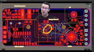
At 35:40 - A common mistake, to match a differential pair with a squiggle 'somewhere' in one of the two signals. THAT SHOULD NEVER BE JUST SOMEWHERE IN THE MIDDLE. The pair is meant to be fully differential, and creating a length jump this way is like a phase jump. This means that at least on one side of the squiggle the pair is not balanced. The skew correction in a pair MUST be near the cause of the skew, e.g. the sideways leaving of a BGA pin pair.
Yeah I was curious myself how those lengths, which are most certainly inductors, would effect phasing and whether that would cause problems of their own
@@xxportalxx.: Don't see them as inductors, they are transmission lines. A delay is inserted by the squiggle. My use of the word phase was misleading. The problem here is that a differential line must have both signals complementary with the same timing, if not noise emission or reception may occur. The skew at the receiver end between the two signals must be zero, or else the differential signal will not cleanly change over between + and -, but will be zero for a a short time. The behavior of the differential receiver is undefined for zero input, and even double clock edges might occur after the receiver.
@@ariedemuijnck hmmm, high frequency stuff isn't my forte I admit. My background is more power and physics so I couldn't help but think about phasers 🤷♂️
What happens when the squiggle is misplaced, see this awesome computer simulation ua-cam.com/video/ZyoqhJB_E9Q/v-deo.html&time_continue=1192
Not exactly sure what you mean by the 'cause of the skew'. Can you elaborate a little for the uninitiated?
Back in the day ... :-) I worked with an engineer that needed to delay an NMI signal to be slightly after the rising edge. He used what he called "Mickey Mouse Logic", placing 4 unused inverters in series between the source and target. It worked flawlessly at 1 Mhz. It was a bit eye opening for me at the time (I was like 19 or so), and has stuck with me ever since (this was in late 80's or early 90's).
Yep, very common delay technique. Also useful as a bodge on production boards if you have spare gates
@@HaseebElectronics Almost 14 minutes to show how to use a crimping tool. I don't even I could make it that long
@@EEVblog lol. Brutal honesty.
i might go look at that crimping tool vid...oh hang on..this guy has spammed it on a bunch of comments here....screw his spam!..his channel is now added to the block list!
I've heard a great story of someone who patched a gigabit phy onto an ARM-based SBC (for prototyping/validation purposes prior to custom design), replacing its 100Mbit phy, since all the signals were there. Unfortunately RGMII has an annoying requirement that the PCB needs to add 1.5-2.0 ns of delay on the clock lines (unless either host or phy supports "internal delay", which wasn't the case here), so he just used 60cm patch wires for those two signals, problem solved! :-D
I still think it's a terrible crime he didn't take pictures of this monstrosity.
wow, I have to admit I don't understant much, but realizing how complicated PCB design can be is already a valuable lesson. Thank you for this one Dave!!
Very informative Vblog, I hope you will have more in-depth videos about signal integrity and DDRs in future.
Amazing content! I am starting with SDRAM and this kind of crash-course video is invaluable. It is not only about the knowledge, but more importantly about understanding the whole scope of things we might not know, as well as the relative importance of them. Please continue.
video about how to read a timing diagrams is a great idea.
Trap for young players is to route busses on different layers.
Make sure to use exactly the same vias for each signal of a group. That way, manufacturing tolerances have no effect on your length matching. They all change together.
I just had to route a 16-bit DDR3L memory to an FPGA on a 20 x 20 mm PCB. That was NOT easy. Big boads are so much easier. Especially for length matching and crosstalk.
The example design shown in this video did not look great in that regard.
Loved the video. Please do more like this. I'm a student at the University and I want to get in to that short of stuff.
Interesting stuff. Yeah an in depth memory timing video would be great. Keep up the good work :)
Yes do a video on the timing diagrams. It took me forever to kind of understand what was going on with those and I would love to get a better understanding.
Yes please! I'd love to see your in-depth tutorial for reading timing guides! :)
I'd really like to see a video on those timing diagrams :)
Second that!
I'd love something on timing diagrams Dave!
Propagation delay was an issue before many folks were born. The CDC 6600 used a backplane comprised of a mat of twisted pair wire ending in taper pins. Seymour Cray tweaked the lengths until things worked. One of my managers had the task of measuring the wires to which Seymour had attached a tag that said "TUNE", so that they could be used for the production machines. The clock for the 6600 was a blistering 10MHz.
Even before that, Grace Hopper used to pass out 1 ft. lengths of wire to her students, identifying them as "nanosecond" wires. (Light propagates at about a foot per nsec).
How on earth do PC motherboard manufacturers manage to turn around these hugely complex designs so quickly? Imagine all the layout time, testing of the DDR4, PCI, SATA, NVMe, USB3 etc. And then charge less than £100 for them. Amazing.
I guess they have very sophisticated tools built over decades to help them with the process. But it is a very complicated thing to do.
lots of copy-pasting, industry-specific tools, decades of experience
@@redtails yes, Intel, for example, release reference implementations for some parts of the mainboard design. The companys can also internaly more or less copy and paste between different boards and generations and switch out only the parts of the design for the new stuff. An other advantage is that they can split the development costs between tens of thousands of boards.
It really is incredible the engineering that must go into them. That, and even video cards. And then you consider the typical life cycle of these things. you're lucky to get a few months before another version comes out, it's crazy all the work that goes into it for such a short life span.
I agree, PC motherboards are some of the most intricate PCBs in consumer homes today. Advanced EDA tools, 24/7 PCB design/layout shops, design reuse, offshore manufacturing and economies of scale result in these marvels coming out so quickly and inexpensively.
Love you take an Argentinian project as example, we are proud of our engineers. Thanks you very mutch.
Thank you for geting us through this rabbit hole. Plenty of info to think about.
Yes, please, please, please. Do N-hours long video about signal integrity. It's fascinating topic.
What I learned today: "You wouldn't want to go wigglety pigglety"
Yes!
And all this for Mhz-level signals, imagine the headaches designers have to go through for the current Ghz-level motherboards !
This is why things like PCI Express came about. Instead of having wide busses to match you just have a couple traces running at much higher speeds. And then for the PCIe x Lanes each lane operates somewhat independently so that matching between the Lanes isn't quite the concern. All this makes for much tighter requirements but with far fewer traces to control. DDR is one of the few high speed parallel holdouts though there have been attempts to move to a high speed serial interface for memory - I'm looking at you hybrid memory cube.
@@slashdevslashzerolots of things are moving to this serial lane idea now. Ghz ADCs these days use JESD204B which is a high speed serial interface, so for a 500Mhz adc, you might have 2 serial lines running at data rates of 5Gig each!
Things like thunderbolt use serial lines too, so high speed design isn't going anywhere!
please elaborate, I guess you use HyperLynx everyday
Another golden content! Thanks Dave.
I will pay for a video series on this topic that covers all aspects of it. As long as it is reasonable.
Thanks I would love to see a series of videos on this subject. There was a lot material to absorb and I’m going to need to watch this one over again and then possibly a third time after that, or maybe four.
A Video about signal integrity for high speed signals or differential pair impedance would be great!
"A video about signal integrity for high speed signals or differential pair impedance would be great".
-Daniel Lang, 17 hours ago
I think the Er will also affect attenuation, so that's why they will bother in RF, not just related to propagation delay.
Sorry, Dave. I think you made a reservation at 32:52 minutes, not 7.5 mm, but 4.5 mm. Thank you for your lessons, they are wonderful!
a video about timing waveforms would be amazing!
Top quality content as usall thank you very much Dave
Do more videos like that. It was really informative. And do the one on timings.
Watching this in my phone and now it feels like im holding a piece of black magic in my hand... man we take so much for granted
I'd love to see a video on timing diagrams. thats a great idea :)
All these 180° bends, must be an absolut nightmare for the busdriver.😂
Amazing stuff. I didn't get where I am today by paying much attention to PCB layout. I just designed the circuit (taking into account sample and hold times), and somebody else laid out the board. It usually worked.
More of this, this is great content!
@18:19 , Dave, please make video on how to read timing diagram, I want to learn from you.
This topic has come at an interesting time. I've been fiddling with some laser driver and TDC circuits to make a lidar measuring tool, and have been learning more around the topic of propagation delay. More so in picosecond TDCs. I found an interesting topic on using FPGA's, to run a clock signal through a series of single gates, to take advantage of the propagation delay, offsetting an array of clock signals all in parallel, each running to a counter. Then you trigger a start/stop signal across all the counters, and determine out of the number of counters, which counter does the increment decrease by 1 You now have 1/x the resolution of your time. Interesting stuff, but I'm sticking with a TDC7201 for now, FPGA's, project for a later date.
I have the education/development edition of that board :) Greetings from Argentina!
When it comes to memory clocks people are pretty much not aware that what is on the label is often only the data rate and signal clocks not the IC clocks as they've been using clock domains for ages. It is always fun to show kiddies ram from the 80s and 90s.
Aside from my nit-picking comments - Great work Dave, trying to explain this complex matter so clearly and humorous. It shows very well why a 'simple' memory chips needs such a detailed datasheet with a tutorial on PCB layout inside. And an expensive high-speed scope with special probes to verify anything at all.
How much high speed does it have to be?
Love your videos Dave. Thanks. Would you be willing to make a few videos on signal integrity and all the reasons for the mid voltage biasing on DDR memory at some point by any chance?
Has that day come yet?
Also, clock frequency is not necessarily the concern, the major concern is the rise times of the parts. The signal rise times can contain frequency content well above the fundamental frequency of a clock, and if you want to preserve the integrity of the signal you have to consider these higher order harmonics. If you're using modern parts, every trace should be treated as a transmission line if you want to assure signal integrity and good EMC performance.
This is so true. If your clock line its ringing, your single board TTL computer might fail at 1 hz.
this video was so interresting that i activated notifications for you because it was not recommended to me :( the algorithm let me down
Dave set time budget for this video to 40m ±30s and used his video layout software to trim it. 😎
Thank you for interesting video.
Budget was 20min, I blew it.
@@EEVblog It still works tho
Do a series on advanced topics! :D
Helpful information
Most of my current projects are 6-layer boards and I use Eagle's built in trace length tool on any differential signal (such as HyperBus or USB HS) and on any memory bus (16/32-bit SMC for example). In addition, for clock generators such as MEMS oscillators, I make sure there is a ground plane with no interruptions between the XO and XI of the FPGA clock input. Not sure if Dave mentioned it, but even if the clock speed is slower (i.e. 40MHz), the longer the trace, the higher probability of interference which can cause "blips" in the signal and trouble for the logic.
Also, clock frequency is not necessarily the concern, the major concern is the rise times of the parts. The signal rise times can contain frequency content well above the fundamental frequency of a clock, and if you want to preserve the integrity of the signal you have to consider these higher order harmonics. If you're using modern parts, every trace should be treated as a transmission line if you want to assure signal integrity and good EMC performance.
24:18 Aussie kickin' in
And i was worried running usb differential pairs lol fair enough it was long distances;p maybe do a video on that matching impedance and stuff for a budget 2-layer board;p
btw the "snaking" was reduced with more modern interfaces such as PCIe but also more modern DDR4 (or GDDR6) memory as well.
Because there is some kind of internal compensation inside the chips. So you can argue that for example GDDR6 has an 64x1bit Interface and not 1x64bit.
On the PC side I think most of the compensation is on the SoC side with DDR4. Snaking also seems to be more pronounced with T topology layouts.
@@MechanicaMenace Yes, because the "T-Topoloty" is made for maximum frequency with 2 DIMMs per Memory Channel, thus its a bit more complicated than "daisy Chain"...
And, if I understand it correctly, the singal lenth is the same between both DIMMs, while on "daisy chain" boards, the nearest DIMM is the first one to get the signal.
PCIe is fundamentally different because each lane works independently from others (as it's a serial bus, it's self-clocking), so there is no need to match them (you only need to match differential pair). And GDDR6 has x16 data interface - you can download databrief for it from Micron website).
TL;DR KiCAD is great and makes designing 8 layer boards not a pain even if you never designed a PCB before.
The comments already terrify me what people do that layout PCBs for a living. I’m a physicist and I had to learn board design and testing for a board with a large FPGA with DDR3 and PCIe that I needed to decode and measure stuff. It just so happens that this is the most complicated thing one can do in digital electronics but its super easy with KiCAD! The only thing I ever done before is microcontroller-level stuff because the klunkt software always deterred me!!
Splitting ground planes is also a great way to make accidental antennas, or sometimes intentional ones.
Yess finally.
I have no idea how the sbc guys can manage ddr3 layout on tiny 6 layer pcbs!
I tried to route the signals lot of time but so far never been able to length match them!
That board is ddr3 with fly by or something else.
I'm just a guy that have electronics as hobby :)
It's a bit like playing chess - you have to think in advance about future steps in order to avoid routing yourself into a corner. I like that stuff!
Thank you for this excellent video
"Bleedingedge system at daylight speeds or you doing it wrong" xD
That made my day. :)
Great video and please, if you could cover those timing diagrams that would be great!
Great video, thanks Dave. Great way to go ga-ga.
Time to get the super computer running on those PCB designs. Optimal traces coming up...
Awesome video
16:11 "Please excuse the crudity of the model..." Classic BTTF ref! ACK! :)
Good video! I'd love to see a tiny example project for creating a system that uses DDR memory from start to end.
I had an idea some time back about actually creating my own DDR3 memory stick for a PC, and seeing if it would be cheaper to actually make a one-off than buy one.
Robert Feranec has quite a few videos on this and actually offers courses too
@@EEVblog Pretty sure it's never cheaper to make a one-off (even DIY) than to buy a jellybean part.
@@EEVblog If labor is free....maybe. It should definitly going to be more fun to create one rather than buying one.
This video remind me of funny (not) case in my life... I worked as repairmen on old (late 70s early 80s) telecom equipment in early 2000s and our job was to repair it after catastrophic PSU failure (PSUs was replaced with new ones after, its obvious thing to do).. The issue was found in CPU (contains ALU, CPU registers, System bus buffers, and Clock generator) card and it was replaced with spare but system worked kinda funny(not work at all) after that. If you run ALU/ROM/RAM/IO Registers tests - it works just fine. That was hotspare dual machine setup where second machine do checks on first one and copy its registers and RAM states over by timer or external trigger like alarm or operator's command. Same for first machine and depends on selected Master machine between two of them. Well. Second machine running, operator gives command to first machine to seize master role. It gives ACK and start to run equipment. After 20 to 30 seconds second machine seizes master role and halt first one. WTF? Operator run tests - result: All Green. Repeat tests - result the same. Operator tries to pass Master role to first machine again - it works but situation repeat itself after 20 or 30 seconds again. We knew for sure that issue in CPU card itself because everything else is tested and works before so it's time to dig in =). Issue was found in "Known good" card, in "Stem Clock Output buffer" chip - it was 4AND gates chip that just its function name said - output 4 equal clock signals to Stem (system bus) that connects Branches (commutation matrix parts) to the Root (CPU shelf). Some bright head replaced SN7408 IC with 74LS08... Good fast and sharp clock pulses generated by 74LS chip was too good for the rest of equipment and glitched out the rest of SN74xx based system bus controller that was in different enclosure about 50-60cm away in the CPU shelf... and yes, that equipment had wire-wound backplane too.
P.S. If someone reading this turd to this point - sorries for broken english xD And I like very much that "Plants" terminology applied to telecom equipment...
Северный Зверёк Nicely and well written post, except that it's "terminology".
@@johnfrancisdoe1563 lol. Thanks for pointing it out.
We tried to keep 7h (for uS) and 5h (for SL) serpentine spacing when length matching the DDR signals. That is to minimize the self inductance. Memory is the most challenge part in motherboard layout. Need to be careful of the RelativePropagationDelay and StaticPhaseTolerence :-)
That was the reason why AMD disabled the PCIe 4.0 (double the speed of 3.0!) in the last gen MBs
They said that the signal integrity would be bad and that would causes instabilities.
The new X570 are designed with PCIe 4 in mind with tigther timings and better traces routing
Question from a bit out of topic: What to do with working DDR-2/DDR-3 modules left from RAM upgrade in PC and laptop? Like 512 MB and 1 GB ones. Throwing them out seems a bad idea.
I think I've seen PCB weave at 45 degrees to the tracks on some expensive 80s test gear and now that makes sense.
I would be interested to see a video on those timing diagrams. I just couldn't workout why a Dallas DS1220AD NVRAM was not working on a arcade PCB, but a ST M48Z12 worked perfectly. They are both listed as compatible items for the same SRAM chips. From what I could see the dallas was stuck in high impedance to stop data corruption.
At these frequencies, wouldn't 90° sharp bends in traces cause problematic signal reflections? I notice the tool has apparently made a few sharp corners near squiggles.
Once you have routed such a high-speed-board how is it typically verfied (in industry)? Just switch on and see if it runs?
Ive routed DDR3 in KiCAD, it worked out well but was a major pain to figure out the necessary length relationships between all of the lines.
Hi Dave. Good video again. Just a quick note to let you know that jaycar now have a new item on their catalogue you may like. It’s a little pricey though. A flux capacitor!!
Nice video ... can you do a follow up video on DDR5 which does away with the need for matched trace lengths, it uses some fancy pants adaptive interface training for timing traces on startup.
16:20 You should probably have warned that this trick does _not_ apply to the address lines of SDRAM (both SDR and the many generations of DDR) which absolutely *do* have to match up since they're not just used for memory addressing but also for mode register programming and for some additional control signals during column select.
Hmm suspicious... ;-) ..., Dave works on a GigaTron-X Mega or something. First a redesign of the board and now a TTL DDR topic. Gotcha!
Of course the trace length matching doesn't just stop at the BGA pad either. IIRC the chip manufacturers have details of the trace lengths for each signal on the BGA PCB too. I think there was a talk someone did about doing that in Kicad with the python integration but unfortunately I can't find it.
I wonder, whats the wire length of a wire wound resistor typically? Never seen that on a datasheet, is it something you'd have to consider?
they make cross wound resistors that have lower inductance. but a regular wound resistor is also an inductor. So it's not a controlled impedance.
I have really always liked your videos, and I think that, among many channels that tackle aspects of technology on youtube, you deserve cudos for, more often than not, having something actually interesting to say about subjects pertinent to the electronics design and engineering, however, having already built your audience and established your presence, you should not feel too compelled to speak fast and nervously, filling all possible spaces with redandent utterances, especially, that you easily have enough personality and valuable things to say, to do exactly the opposite, and not be putting yourself up for verbal contests, with fast and easy talking lipstics, soaps and facial creams retailers. Thanks for valuable content, but for even better results, consider this: words carry weight.
I think you used too many words...
@@EEVblog Thank you for sharing your thoughts. Your vlog is, in various aspects, a display of artistry with priestly and humble relation to knowledge. And so, I hope, that my previous comment, while not intended to be excessively assuming or verbose, gives away nothing, but just that impression, of well deserved, appreciation !
Remember, PCB vias can produce reflections, influence the speed and trace impedance as well. Vias can reflect and act similarly to distributed element filters.
Generally, stacked microvias are a bad idea hehe
Wow, all these issues ring just as true when laying out datapaths in digital CMOS (say, on a custom DSP). Only, when laying out ICs, we're regularly operating in the tens of picoseconds domain. There is a whole field called Static Timing Analysis that unsurprisingly deals with timing analysis for digital VLSI designs.
Can Vref cross-talk be overcome with judicious use of grounding caps at each chip?
What software is Dave using to show the routing here? Is that a viewer application?
This is good stuff.
At 24:53: No, skew is the difference between propagation delays, not the same as propagation delay.
Fascinating
Great double data rate mate
Haseeb Electronics Chowk Azam Hahahaha good one!
I worry about a product where we did not spec control impedance. we measured the pcb by making a long trace and used that for the 1gb Ethernet traces and the traces for the phy.
hi Dave, would you consider using Ublock Origin? An opensource, better alternative to that other Add Blocker you're currently using? Probably it spies on every URL you visit and deffnitely it doesnt block all adds. Just a suggestion.
Great video Dave, but surprised nobody appears to have picked up on your propagation delay estimate!
The speed of light is 300k km sec -1 therefore 1nS = 30 cm at that speed. When I did my electronics degree 45 years ago that was an ingrained measure.
Clearly electrical propagation is not as high as the speed of light, for various reasons, but generally taken as between ~65% and ~80% depending on exact medium and circumstances.
Safest rule of thumb is therefore to use the speed of light rather than half that, thereby ensuring a good positive margin for high speed circuits. Not so critical at 100 MHz obviously but significantly more critical at 4GHz, or above.
I can smell ham.
@@BenMitro what flavour? 🤔
@@boblewis5558 that depends on the country you are in Bob. I just got my advanced as we call it here in au, waiting for my call sign allocation.
@@BenMitro wasn't aware the speed of light varied by country, certainly not by a 100% increase or 50% decrease! 🤔🤔🤔
At 32:50: "Let's get the confuser out again". How true. You use 15 cm/ns times 50 ps - that should be times 30ps, leaving you with only a 4.5 mm skew margin. When we designed boards like this we stayed well inside those margins, and they worked first time right. It is doable...
When something says that it wants a controlled impedance differential pair - how important is it actually?
I had a look at USB a while back and it wanted 90 ohms impedance for its D+ and D- traces, which led me to look up what that actually even means. It looked fairly simple, as long as you don't need it spot on. (I think it said you have a 5% margin of error, if I remember correctly)
Now, if the traces are very short, does it still matter? How important is it, that D+ and D- actually have the same length? If you snake one but not the other, you end up ruining your differential pair somewhat.
Just try it, hope for that best, and go back to the drawing board if it doesn't work?
On that note - what does actually happen if the impedance is too far out of spec? Does the signal degrade to the point it just stops working?
For usb it is important. But to be fast, keep the track length under 1cm and you'll be sweet. If the impedance is wrong you get all sorts of great reflections and they can make life hard. USB will not tollerate much noise on the transmission line, so dont make 10cm usb tracks pass over anything oscillating. Keep them short as possible and then you dont need to think about it.
The Gigitron TTL computer is very slow compared to modern digital electronics. Its effectively late 70s & early 80s technology. HC TTL gates has probagation delays ~30nS. F series down to ~3nS. PCB layout is irrelevant as far as propagation delay is concerned. Timing diagrams are still important. Due mostly, to how slow the devices operate. The TTL logic was the faster part. It was the slow NMOS LSI chips (microprocessor, controller chips, EPROMs, etc) that had to watched. EPROMs had access times of several hundred nS.
The following is a project I worked on in the early 80s:
threeneurons.files.wordpress.com/2019/01/esz7000.pdf
Look at page 4. The board looks a lot like that TTL computer board. Same technology. Used a 4MHz Z80 processor. I used timing diagrams all the time, back then. Again, because, how slow those old memory devices operated. Wait states was a common thing.
Dave was a teenager in the 80's. I was already a 20-something working engineer.
I had some Corsair DDR2 1066 that was just not entirely stable at 1066 on a ASROCK N68C-S UCC. Sometimes it would mess up during the initial temperature changes. The gigatron at 8Mhz though, like the DDR data would be there like RIGHT NOW but really would idle a lot. I am sure you could slow it down a bit and take out any problems.
30:31 Why does increasing the trace width reduce the inductance?
Not sure, unless he meant impedance. This is a little above me so I could be wrong.
When a current flows along a track it generates a magnetic field around the track. The magnetic field lines run across the width of the track around the edge and back across the other side. If you increase the width of the track it increases the length of the lines. The inductance created by each line is inversely proportional to its length so increasing the width reduces the inductance. Another way to look at it is to imagine two parallel tracks of half the width, each having inductance L. When you combine them into a single track with twice the width you are effectively connecting two inductors in parallel which halves the total inductance.
@@petehiggins33 Thanks, that's interesting.
The next logical step past QDR would be six words of data in each clock cycle, by adding a third double data rate clock, but what would it be called? HDR is taken :P
Rule of thumb: If the trace is longer than the wavelength check the layout in an EM simulator.
Hey dave, any chance to take a look at the new 8-bit computer that the 8bit guy wants to do?
The 8-bit guy don't want to use such 'modern' stuff like DDR ;-) . He really likes to reinvent the wheel with some extra's. Have you seen the latest board design, it is huge and expensive, doesn't fit the few tens of dollar price range he had as goal. You must be nuts to buy such system for only a little extra memory and a little more powerful graphics card. 8-bit guy was thinking of his dream computer with 8-bit-guy limitations because the 8-bit guy assume you don't need more, because the 8-bit designed it. It is not Apple and not a game! A fixed device you cannot configure or change, who else wants to buy this thing anyway?
There is already an open source FPGA version of what he want (reviewed by RetroManCave), others did the hard work and because it is open source he is able to download it and change the design. But he doesn't want to use a FPGA (he also noticed this in his last video), must be off-the-shelf parts with all the extra effort and costs because it must be old-scool in every manner. The FPGA used in the open source version is an intel, maybe that isn't his cup of thea.
I dunno........ Dave, take a look at it, what do you think about it?
Video 8-bit guy: ua-cam.com/video/sg-6Cjzzg8s/v-deo.html
Video RetroManCave: ua-cam.com/video/e5yPbzD-W-I/v-deo.html
If you're going to use an FPGA, might as well just emulate it and be done with it.
@@gblargg No you can not.
Because FPGA basically the original Hardware or something very similar to that. And the modern ones might be relatively cheap so that you can easily do an old PC with that. Look at the FPGA Nintendos! They are pretty much like the Originals, more or less.
Not much point. Eventually, they'll realize that the parts they're using aren't going to work out, and they'll have no choice but to put everything other than the CPU and maybe the VIA into a single FPGA. Even then, the original goal was to use as many "off-the-shelf" parts as possible, yet it now uses dedicated video ram, supports multiple graphic layers, dozens of sprites, 256 colors, 2MB of RAM... uh, this is supposed to be an early 80's computer, right? Sounds more like a 32-bit machine running off an 8-bit bus just because. The Mega65 has similar issues. These machines are too expensive and not at all representative of the 8-bit era.
I'm working on my own 8-bit machine, but I'm thinking about it at the gate level. So, even if propagation delays at the PCB level don't matter, the delays of the gates in each custom chip must be considered. It'll only be simulated in software, since I know nothing about FPGAs, but I want the features and specs to be realistic enough so it could theoretically be manufactured at 5 micron HMOS. I think that's way more interesting, fun, and a serious engineering challenge, than slapping a whole ton of features together just because a modern FPGA has enough room inside.