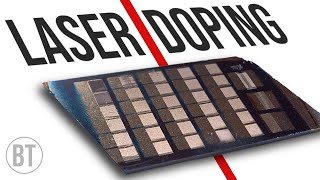
Laser cutting Silicon Wafers

Вставка
- Опубліковано 23 лип 2024
- Micromachining silicon with lasers (but no sharks)! Today we're exploring different properties and parameters involved with cutting silicon with a pulsed nanosecond laser
🥰 CONSIDER SUBSCRIBING 🥰
🔬Patreon if that's your jam: / breakingtaps
☕Or buy me a coffee? www.buymeacoffee.com/Breaking...
📢Twitter: / breakingtaps
📷Instagram: / breakingtaps
💻Discord: / discord
==== Links ====
- Photon sieve design is from: Andersen, Geoff, and Drew Tullson. "Broadband antihole photon sieve telescope." Applied optics 46.18 (2007): 3706-3708.
- Experimental watch oscillator is from: Thalmann, Etienne, et al. "Flexure pivot oscillator with intrinsically tuned isochronism." Journal of Mechanical Design 142.7 (2020): 075001.
- Big watch flexure is from: www.thingiverse.com/thing:453...
Some videos about nanosecond etching, cutting, drilling:
- • Cutting and Scribing w...
- • Drilling with ns Pulse...
==== Timeline ====
0:00 Nanosecond laser
1:00 Why silicon?
1:46 Examples
2:32 Tip #1: Polished vs unpolished side
3:10 Tip #2: Focal length
4:00 Tip #3: Heat management
4:40 Confounding variables
5:23 My Best Recipe
5:43 Wobble
7:16 Cut geometry
8:12 Supported vs unsupported
8:57 How good is surface finish?
11:05 Taper in microholes
11:54 2.5D/3D engraving
12:05 Etching interference fringes and fingerprints
12:28 Metal?
12:57 Ultrafast sintering! - Наука та технологія


- As much as I'd love the glitch at 4:50 to be a secret message or easter egg... it was just a weird glitch during video encoding, and I was too lazy to re-encode and reupload. 😇
- Also, I appreciate everyone's concern over my fingerprint, but I refuse to use biometric logins at all (for this and other reasons), so I'm not particularly concerned about it being available. No more dangerous than leaving prints on doorhandles, etc :)
not convinced
are you still going to do a video on telescope mirrors
You created a portable glitch. It's been done.
How much to make me a pocket glitch. Wait. Probably shouldn't put it in my pocket.
Actually, I think that just hit the perfect pixel mixup to screw with encoding. There's a few of these out there that will screw up a lot of encoders perfectly causing these perfect glitches. Also. To your message. I agree. ;)
What glitch?
This feels like a master class's demo of taking amazing SEM/SED photos.
modern microscopes are surprisingly easy to use, its amazing how much can just be done by good software control.
I know I'm not saying anything you don't already know here, but for others watching, the pulsewidth of lasers used for micromachining is EVERYTHING. While we might think of multi-nanosecond long pulses of light as being incredibly short in our everyday experience, they're actually very long on the timescales of atomic interactions and energy level transitions, and so end up heating the material, melting it, boiling it, and just making a mess of things to a significant degree. If you can manage to somehow move into the picosecond or even femtosecond (10^-15s) range of pulse widths, you will enter an entirely different regime of laser-material processing where the electron temperature becomes completely decoupled from phonon interactions at the time scales involved and you can produce exquisitely clean, precise features in virtually any material down to the nanometer resolution level, simply because the material doesn't 'have time' to heat up and create heat affected zones before its converted right into a plasma that's not even touching the rest of the bulk surrounding material anymore. The number of really amazing new things you can then do to materials in this ultrashort pulse regime is totally crazy: creation of ultrahidrophobic and ultrahydrophyllic materials, permanent color alteration of metal due to surface plasmon resonance tayloring, near perfect blackbody radiating surfaces to dramatically increase incandescent filament efficiency, etc. If there was some easy way to modify a ytterbium fiber laser for short pulse operation you would be able to do vastly more with it as a general tool. Maybe frequency doubling it with a piece of nonlinear crystal could allow other more subtle material processing too?
What do you mean increase black body radiation? Like making stealth coatings.
Do any lasers do this now?
@@ohbeardedone9253 yes. relevant paper was in PRL
"Brighter Light Sources from Black Metal: Significant Increase in Emission Efficiency of Incandescent Light Sources"
yeah, that's why we always had to use mechanical or chemical to machine at some point - laser is easy but in submicron feature creation it leaves tapered holes/edges especially if you're trying to slice tiny precise cubes...or dice a wafer. To this day it's done nearly completely mechanically. Grind and saw.
you're describing something that seems to be live correction of lithography and honestly that's very small scale (feature wise) and the actual models already exist (it's just restricted to process engineers who stand on the shoulders of the PE's that came before them) but in more practical applications of, say, "garage" use there are pretty awesome spherical and liquid lenses that can be tuned spectrally as well as refractively. I don't see why something like a ferrofluid couldn't be used in a set of rings that could deform a squishy lens with not only surface topological features but vary the density of the lens material itself on the fly. As usual, the biggest hurdle is addressability but somehow if you cock your head just right it always seems to present a method. Rings with rings. Zebra stripe edges but large toroids of them. Depending on what part of the lens you look through you can wrap it pretty much however you want as long as the optical transmission path to the target is unobstructed.
That's discounting quantum imaging, et al, but that's both way off the path or one of the ways to the truth. That's the thing about it, I guess.
maybe if we figure out how quantum imaging works, we can quantum machine materials.
make something without ever seeing it.
actually, the two methods below use the same imaging configuration (note they continue using the two terms interchangeably - that's why WP is irritating sometimes). there is simply no consensus on how it is actually doing what it is doing even though in one study it was able to detect an object simulating breast cancer in an actual chicken breast without even looking at it directly using eyes or any known method of detection. it's merely sorted itself over the past 15 years into these two loosely coupled buckets.
From WP (links tend to get scrubbed by YT autobots):
Real-world applications
As research in quantum imaging continues, more and more real-world methods arise. Two important ones are ghost imaging and quantum illumination. Ghost imaging takes advantage of two light detectors to create an image of an object that is not directly visible to the naked eye. The first detector is a multi-pixel detector that doesn’t view the subject object while the second, a single-pixel (bucket) detector, views the object.[12] The performance is measured through the resolution and signal-to-noise ratio (SNR). SNRs are important to determine how well an image looks as a result of ghost imaging. On the other hand, resolution and the attention to detail is determined by the number of “specks” in the image.[13] Ghost imaging is important as it allows an image to be produced when a traditional camera is not sufficient.
Is this a retroencabulator comment? I feel like half these words aren’t word
Some glass cutting lasers work by ablating a series of small holes only part way through. They then wait a few minutes for the stress cracks to propagate between the holes. You might want to try that on silicon.
Oh interesting, that's a neat trick. Will read up on that and see if I can do the same.
The cracks will tend to follow the crystal grains. That said, there is a thing called laser assisted dicing you might want to look at, but the curves tend to be larger radius.
Yes, show the interference pattern. Would have really wanted to see it under the microscope!
This might be a good way to make custom diffraction gratings too…?
8:10 Did you though about making support out of... needles? Like water jet/plazma cutters have those spiked tables, but just tiny little ones. Like getting wood/plastic base and stuck on it bunch of needles.
Ah, that's a clever idea! Will think about a way to set that up
@@BreakingTaps Yes! I was just about to comment this idea. I was thinking, instead of a uniform bed of needles(where maybe important parts don't get supported or you risk hitting a needle), maybe plan strategic needle support points and you could burn holes for needles, or at least burn pilots to drill holes to put the needles. Very exciting capabilities on that laser regardless! You've got another subscriber!
Can't remember where I saw it, but someone was making cuts on tempered glass (I think?) by submersing it in a very shallow water bath to handle heat. It worked surprisingly well. Might be something worth investigating here as well? Surface tension might help give a small amount of structural support during the cut too. Awesome results either way!
Might have been Applied Science I think?
@@RamiSlicer that sounds about right!
I came to the comments to say this, then came to the answers section of this comment to supply the name of the channel referenced. Beaten twice by the Internet 🤗
I suspect that may not work as well in this case because the water will change the focus of the laser.
It was applies science, I think he was using a co2 laser to cut ceramic for high temperature circuit boards
Those SEM photos are amazing. I don't know what I would use a laser like this for but I'm betting I wouldn't leave the house for a few months if I had one. Loving this channel though.
Thanks! And yeah, it's a super fun hammer to have in the shop :) I keep finding new ways to abuse it for projects haha
Interesting ,wonder could you dissolve the aluminium with something without damaging the silicon for removal, I'm no chemist, I was thinking sodium hydroxide but a quick Google tells me it will dissolve silicon the same way as aluminium, you could try using a piece of cardboard/paper or something no? Or like coat the back of the silicon wafer in casting wax or some pitch or something that will give it support during the cut but can be melted /dissolved off easily enough
Manual lithography exists - I have never got to drive one but FIB (focused ion beam) die editing is a trip.
I really see this as potential for machining things that are glass and ceramic like, since a silicon wafer (even the reject ones are still impossibly pure and purer than anything found in nature) is, for all intents of handling purposes, very thin glass. Usually they're attached to a sacrificial substrate even after they're diced so they don't get destroyed in processing; final grinds can be highly manual depending on the parts.
But all that being said, there are still a *lot* of methods that can be used in the kitchen to give access to technologies that we'd never get a card key for the facilities in our lives. :-)
There are a few channels here that do a LOT of materials science - I saw a guy go get oyster shells and make a supercapacitor. No lie.
Science is science, the difference between us and the big companies is scale and access to resources. If you can get your own resources (smelter channels YT has everything to teach you) then you don't even need to order out and can of course check your own purity and construction.
Good microscopes are only a few hundred bucks now, if you can get a few hundred bucks together. You can get just the head for under 200 bucks and get a pretty good stereo widefield model. By "good" I mean useful and upgradable...it's amazing how many questions you can answer with that and a 30 buck eyepiece usb camera.
aluminum desolving method could work. In my school's IC lab we use aluminum as the conductors for the mosfets made in our IC design course.
Lasers you say? How long until he goes all Styropyro on us and unveils he used his knowledge to make a death ray?
If you can arrange to irradiate the silicon in SF6 instead of air (about 300 - 400 torr) you can make black silicon. My PhD was on this and figuring out what happens. I used a XeCl excimer laser at 308nm, 10Hz rep rate, ~4J/cm^2 fluence. The ablation, photochemistry, and remelting gives you crystalline pillars forming above the initial silicon surface. They scatter the light so well they are very non-reflective, from long-IR to UV.
Oh wow, that sounds interesting! Is it specific to SF6 (reacts with the molten Si I guess), or just an inert atmosphere? Think it would work with my longer 1064nm wavelength?
@@BreakingTaps I've tried under plain nitrogen and also CO2 with poor results. Seems to need something that can etch the silicon, SF6 worked well for me, NF3 was too agressive and HCl gave some weird results. I know work was done using fs pulsed IR lasers. I can't see why it wouldn't work for ns IR. The trick was to get some Si ablated, SF6 broken down and pump some energy into the plasma to drive some photochemistry. The process starts by roughening the Si surface, this concentrates the light and pits / holes develop where the fluence in high enough, material ejected from the holes is then what goes on to make the pillars.
Interesting, thanks for the details! I'll keep an eye out for a cylinder of SF6 and keep it in mind! Shame a lot of silicon chemistry requires fluorine-based compounds :(
What is the purpose of this? Can you scatter electro magnetic frequency as well?
@@ohbeardedone9253 Features were too small to scatter much longer than near IR.
Wow. This channel continues to amaze me. Brilliant work, and such great clear presentation! Well done
Find a piece of aluminium honeycomb and bond it to a flat surface, it works well as support material with minimal interference with the job.
I also noticed differences between cutting with or without a flat aluminium plate under the piece, I think due to the "heatsink effect" of the support.
I was thinking of machining a spiral into a block of aluminum with an engraving tool with a line spacing of a a few thou. Would balance out surface area and take advantage of the effectiveness of the laser at a greater depths.
As always, really nice to explore with you. Thanks! Having an SEM just changes everything.
I've seen some nice examples of coloured etch patterning with a similar laser, using differential dwell & heating.
For your mounting issues, you might be able to use beeswax or similar, melty compound, on top of metal or granite.
Beeswax is commonly used to fix jewelry to a work surface and releases when heated. I’d imagine that you may have to use a heated solvent to dissolve out the wax for particularly thin pieces.
Or maybe a low melting point metal, like gallium or bismuth. Work with it on a solid, flat substrate and then melt it all off when you're done.
@@Timestamp_Guy Gallium would be interesting for sure. I'd be curious to know if it would wick well enough to the silicon to stick - it tends to oxidize very rapidly and get a skin.
I'm in LOVE with your videos, I comment that a lot on your channel but you just deserve that at least
The projects are so awesome I am almost saving every single video of yours. Not only the projects but the videos themselves are of phenomenal quality just wow
Your microscope pictures are getting really good!
Very cool as expected
fantastic photos of the nanohole array !!!!👍👍👍
Came here for the lasers, stayed for the INCREDIBLE microscope footage.
Great video! Well done!
Amazing work!
super high technology! next level professionality! you have not only a very advanced array of machinery, but your skill set and the way you show and describe your projects...super inspiring!!😃
We use our fiber laser for cutting precious metals. This is awesome to see at a microscopic level! You could try cutting pieces on the fins of a heat sink. Similar to how a plasma table works. That’s how I like to cut shapes out.
Will give that a shot, thanks!
I’d be very interested in seeing your follow up video on producing interface patterns in the material. Has a cool visual effect.
That was fun! Thanks.
Daaaaaamn ! That's some pretty cool stuff !
I love your videos. I only wish these videos had come out 2ish years ago. The topics are perfect.
Awesome work...cheers.
Great video! I'd love for you to go a little more into the interference fringe thing! Looks like a very cool effect, and it'd be cool to be able to think about possible applications (if any)
me too, please!
Please make a follow-up video on the interference fringe thing, that would be so cool.
Also, for the support, could you use something like wood, that can't be welded, or something with a really high melting point, like tungsten to prevent the sticking? Or just use an anti-spatter coating?
agree...this looks quite interesting...
When using a similar setup in our lab we use a kind of ceramic to support. I'm not sure which but I imagine it will solve your welding to the support problem
This is so awesome!! I'd LOVE to have one of these one day..!
So cool!
Those micrographs are beautiful. I feel like they're getting better and better with each video.
Thanks! Slowly getting better at taking them :) There's definitely an art to it that takes some time it seems
4:50 Glitch alert! I'm only pointing this out because of EEVBlog's recent video about similar problems with glitches when filming silicon wafers. (WEIRD Blackmagic ATEM Mini Fault)
Oh, weird! I saw that glitch last night but decided I didn't care enough to reencode and reupload, I didn't realize it was a "thing" though. Will go check out EEVBlog's video about it, super strange!
@@BreakingTaps Might be for a completely unrelated reason to be fair.
Came down to the comments because I spotted it and wondered what it was. Thanks for the heads up about the EEVBlog video.
When I first saw that glitch, I thought it looked like some kind of bar code. If it only appears on films of silicon wafers, maybe that's really what it is: some kind of tracking number only visible under the right conditions.
One of the coolest videos I've watched in fifteen years.
It beats cat vids, hands dwn.
Your videos blow me away every time. It is so pleasing when art is an emergent property of science. Trying to find two humble cents to contribute... have you tried floating the wafer on a dense liquid for support and heat dissipation? Maybe molten bismuth, for instance.
yes show us the glass diffraction and thumbprint process
Wow the micro hole array was so interesting to look at
For our laser cutting machine we use a borofloat pane as a substrate; we also place the focal point on the back surface of the material. We have a 2mm focal depth, however, so I don't know if this may also help with your machine.
certainly a theme with lasers lately but that is definitely not a bad thing!
When you've got a hammer... 😁
Thank you for using flexures! I'm super interested in this stuff but it doesn't seem to have really gotten hold of youtube makers and experimenters. I have read the paper on the watch oscillator but hadn't found the 'big watch flexure' so thank you for that!!!! it's going into the Fuse 1 right now⚡️
Oh awesome, goodluck with the print! It's a really neat mechanism, even if I have no idea how it works in a watch 😂 I bet it'll be awesome SLS printed!
Very interesting!
Goddamn! Thank you for your work 🙏
could you place some kind of wax layer between the wafer and the aluminum block used for support in order to glue the keep the part stationary and supported and then melt it to get your part?
I was wondering the same. It would have to be a material that does not generate a burst of gas when the laser punches through and hits it because that would likely cause the work to move.
Imagine laser cutting your own watch oscillators from silicon
Nowhere else does my mind get blown away in an as satisfying way as your videos.
Great video! Looking forward to a follow up one on cutting metals. Curious to the software you're using for operating the laser, I'm used to using EZCAD 2 though I'm unaware of how to program multiple passes with a specific delay in between.
This is cool! Something I would love to try some day... Just have to build my micro-lab up now... Maybe I will send a quote for an AFM to start with.
You could try using a dissolvable support material.
Oooh! Man, you have the coolest toys!
Impressive!
*engraves fingerprint*
"Dont know what that would he used for"
**mission impossible music plays in the background**
Yes please do the video on the interference fringes/fingerprint :D
You just made me remember micro machines from when I was a little kid! Anyone else remember those?
Man I loved micromachines. I had the unfolding toolbox city thing and it was rad
wow Lasers are awesome
I've been running a 1.5kw industrial fibre laser for about half a year, so all this is familiar, yet new and interesting. I've managed to get some pretty fine detail for such a large machine (0.2mm wall thickness), but nothing like the small galvo-mirror type machines. Some of the big machines are now incorporating glavo mirrors into traditional gantry-style cutting heads for "wobble"-like features. I wonder if some of them will eventually be able to offer the best of both worlds.
You could try doing a post-processing pass without wobble to clean up the edge. You may adjust the path to "grind" into the imperfections (ie.: printing at 99% scale).
For the issue of supporting, could you cut them on top of a soft material, maybe even some sort of foam, that would just burn away when the laser breaks through? If you ever would need to make a lot of identical pieces, you could CNC out a base that has a sort of "shrunken" version of the final shape beneath it, but the edges offset a couple mm so as to allow for a space for the laser to go.
What happens if you spin coat a thin mask material on, use a single pass to ablate the mask, followed by a deep anisotropic etch?
The mask could be a melamine type resin rather than an intentional photoresist.
I believe it should work! I've seen similar done in the literature, and as long as the resist isn't etched I think it should work fine. I've ablated away thin metal films in the past so a polymer wouldn't be a problem
@@BreakingTaps you can also vapor polish it pretty easily, saw a guy do it to acrylic - chemicals are great for controlling a coating or layer of additive or sacrificial material. Might have to get residue off but for just a lab test for developing and understanding your own processes in the context of what you want to build it shouldn't be any more excessive than soldering as far as toxic waste.
KOH anisotrpically etches Silicon. As to a mask, one might be better off using oxidized silicon and a CO2 laser. CO2 will etch the oxide and not the silicon.
For cutting acrylic on a co2 laser it's common to use a film of dish soap to keep the redeposited ejecta from sticking. Wonder if that would work in this situation as well?
Could you please explain how you engraved the interference pattern from the glass?
Very awesome video!!!❤️
Hey, was just thinking, that looks like it's vaporising a not tiny amount of silicon and making oxide and I'm guessing it's super tiny and dry. watch out for silicosis from it buddy.
not that I'm expecting a giant risk, but it might be something to look at/think about.
other than that, what an Awesome project.
I really want one of those lasers now lol
Agreed! I was wearing a respirator and had air extraction running to help capture the particulate. Probably should have mentioned that in the video, whoops!
@@BreakingTaps all good mate, it just struck me as one of those second order type deals that can come back and bite you. Glad to hear you're on the ball. Mentioning the non obvious risk for anyone who replicates is probably a good thing.
I doubt it’s a huge risk. If I remember correctly silicon is only dangerous from 150-2um. Below that, which this certainly would be passed right through all membrane in the lungs
Water jets use a ribbing system to support the material. Maybe you could also use some form of wire pin cushion. Like a wire brush type platform.
Can you share any other info on your laser setup? I want to get a laser for the shop in order to replicate some of your awesome videos but don't know what I should look for.
Thank you for the video. Which laser system (Power, Make, Model) did you use for making those structure?
WOW!!!!!! Thast all I can think of... just WOW...
Thanks for sharing this very interesting application and I cant wait to try this on my machine. I have a 30W fiber marking machine. What power is the machine you used to do these parts? Cheers
I know someone who runs a nanometre lathe making tiny cones for microwave electronics
Apparently the trick is turn the inside in aluminium, plate it with copper, turn to size then dissolve out with acid to remove the ultra thin wall part
This video made me think it might be interesting to your projects
Hey, I run a CNC laser cutter at work (macro, not micro). There's the same problem of support/welding at a larger scale, but there's also a solution - slats. We use slats with teeth to further reduce contact with the workpiece. Perhaps for your use case, you could cut micro scale slats out of silicon?
Knowing that there is a Photon sieve Blew my mind.
I was like "YOU COULD DO THAT???!!!"
Интересно увидеть какой то микро механизм работающий. Часы например. Круто !
I wonder if I could use a diffraction pattern on frosted glass slabs to use as a working surface that just sort of soaks up the overflow without destroying it.
for me the most intriguing results were those non mechanical parts like the photon sieve and those interference patterns.
do you think there's a better material to cut those into? will literally paper work? paper with an interference pattern or a fresnel lens in paper sounds awesome!
Paper doesn't like my wavelength much (and/or catches on fire😅). Metal might end up working best just because it's a little easier for the the laser to manipulate without fear of cracking. I've had pretty good luck with carbon steel shimstock so far. Still experimenting there so hard to say. Also easier to cleanup without nasty stuff like HF :)
I'm surprised Applied Science isn't commenting on this channel. Usually when I find channels like this he's already here
To manage the heat cracking the crystal you might could cool them from the bottom. Maybe it would create a worse temperature gradient and they'd crack even more, at which point you go the other way and warm them up so that the lazer doesn't cause as much thermal stress!
Laser cut a silicone support structure that resembles a plasma table support to cut silicone on.
Could you use some sort of needle setup for support?
Hello,
I need to do this exact thing for customers. Can you give me more information on the type of laser you are using. I get so much conflicting info on the web and want to make sure I purchase the right machine the first time.
Thanks
I wonder if there’s a way to support the part with a chunk of glass / lens that would defract the laser, or if silicon and glass don’t play well together then something else that would defract the light energy on contact.
Would it be possible to model in software the thermal behavior of the sillicon piece, and adjust the g-code for optimal cutting time with the smallest risk of damage by uneven expansion?
Coming soon breaking taps first cpu
Would you mind sharing your ezcad files for these designs? Want to see if I can replicate some of these. You are doing an awesome job with this channel by the way. 👍
What about supporting big parts with lots of small needles or thin pillars or something? If you can get them to the same height I feel like that could work
Oh man, I would love to see you make one of those silicon wafers into a super epensive record disc by laser oblating the tracks into it!
Hah, that's a fun idea! Gonna have to think about that. The laser part would almost be the easy side, it'd be the reading and electronics on the other end that would probably stump me :)
What settings do you use on the laser? I have a similar laser but can't get the settings right to cut silicon
Any idea on how silicon watch springs are manufactured?
is it possible to use this laser to etch the inside of a glass marble or sphere?
A potentially cheaper alternative to dynamically focusing beam optics might be to use one or more of those JWST mirror adjusting mechanisms to move the stage up after each pass. It might require more precise motion control than the adjustable focal plane system, but it would avoid having to modify your laser and also not require buying more optics hardware.
Would a graphite block work as a support structure? I know it can stand high heat but I don't know if it plays nice with lasers?
could you use a masking chemical of some sort on the support material to keep it from welding?
another (possibly quite expensive) option might be to support it with an aerogel.
Possibly! I think it'd have to be pretty thick, the molten splatter that comes out the bottom is probably pretty violent.
Have you considered using PMMA as a support and etching it away in acetone?
can the microhole arrays be used for schlieren-photography/a similar concept?
can you make color prints where color is achieved via diffraction patterns?
I haven't personally been able to "dial in" a specific color on metals yet, although I know some folks with fiber lasers can do that. MOPA lasers make that a lot easier but I don't have one. I can fairly reliably make the "rainbow" variety of diffraction patterns though.
Seellll this as a service
9:00 3D printing supports for big pieces. Support pylons would go under piece that must remain. No support material under cuts or where material should fall off. If supports are 5 cm high then when laser gets to them it should be unfocused so no connections between pylons would melt. Maybe
If the right plastic is chosen (like the PVA used for dissolvable supports) it wouldn't even matter if they melt because it could just be dissolved off.
I would definitely like to see how you etched your fingerprint
2:50, u nailed it, we planarize wafers pre-etch to increase quality of the etch (and thus yield in mfg processes). do you have experience in the semi industry? you have such a great understanding and i love ur simplified explanations!
is it a 20 or a 30w laser? kinda looking into bying one, and i was wondering if it is worth it to save the money and buy the 20w instead?
Have you tried oxygen assist, or a graphite backing block? Both are used in larger systems, it may not scale down.
Not yet, but gas/oxygen assist is on the todo list! Didn't think about trying graphite, that's a great idea! Will give it a shot
Wonder how my 60w 2ns laser would work on this. My laser also has a powered Z axis that adjusts down as I cut.