I'm sorry for such a repetitive comment, but I need to say: thank you for your videos. They are fantastic and explained so well. I'm using them to help me in my college class. My professor is amazing but getting two different, well stated explanations is vital for my learning process.
I just have to say this whole semiconductor physics series is fantastic! I´m a physics engineer student from Sweden currently taking a course in solar cells and unfortunately our textbook is lackluster to say the least and our teacher not too pedagogical (not to mention hard to reach due to the current pandemic). Your videos really helps with the intuitive understanding of the subject and they make me even more excited to become a great physicist! Thank you!
EE masters student and have taken probs 8 classes between now and undergrad where the depletion region of pn junctions/devices is discussed and I've never seen a good explanation and this is great.
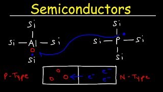
So in Summary, In a pn junction, there are four types of charges, movable and unmovable postive and negative charges. The movable postive charges are located in the p-type and the movable negative charges are located in the n-type. Both types are neutral though due to the existence of the opposing unmovable charges. When the p-type and n-type come in contact with each other, some of the movable opposite charges migrates to the opposite type. As they are traveling, they are repelled by the other migrating movable opposite charges, such that the opposite movable charges migrates at the extreme side of each type. The repulsive field created by the moveable charges contains only the unmovable opposite charges, which are constructs the depletion region. In conclusion, the pn-junction consists of 3 regions, the postive region, the depletion region and the negative region.
Almost. Precisely how I think of it up until the “as they are traveling” part. They aren’t repelled by the other mobile charges (because there’s lots of ions there too balancing them out, so no electric field). They instead diffuse into the opposite region and *recombine*, which is how the ions in the depletion region get “revealed” for lack of a better world. It is these ions that are responsible for the electric field and prevent further diffusion. Far away from the depletion region, the semiconductor is still neutral (it has both its electrons and positive ions, or holes and negative ions). The mobile charges don’t make it very far before they recombine.
Can someone explain why, at 6:06, the electrons on the P-side arent being pushed back into the N side by the electric field. It seems like electrons are only reactive to an electric field on the N-side. Not on the P-side. This doesn't make sense to me.
Electrons moving towards the junction in the P-type region leave behind holes which counteract their negative charge. Similarly, holes moving towards the junction in the N-type region leave behind electrons.
So the diffusion current creates a net charge that again creates an electric field that stops further diffusion? But wouldn't that make the electric field disappear since all diffused charge carriers will recombine and the charge difference would disappear? Is this something that always goes on, but we model it as a stable situation where all free charges are pushed back? I feel like I am missing something or that I've been overthinking this
Yup, you’re precisely correct, except for one subtle point - recombination does not change the net charge in a particular region, as it removes both a positive and a negative charge with no charge - so the E-field will remain after recombination. Other than that you’re exactly correct.
@@JordanEdmundsEECS Thanks for a fast reply! You "destroy" both hole and electron at the same so the net charge stays the same. That makes sense! Thanks again
So can we say that depletion region is only formed by the immobile acceptors and donors which I think you call them ions, which are the ion form of the impurity atoms such as B^-1 for Boron and F^+1 for Phosphorus? and... silicon or any impurity so to say ANY ATOM can not actually move or physically diffuse through the silicon, they are stable where they are, only thing moving is holes and electrons created by them? Isn't hole movement is directly caused by electron movement? When we are talking about hole and electron diffusion, actually there are not 2 particles moving to diffuse to each other. There is only one particle which is electron that tries to diffuse to holes, and the thing we called "hole diffusion" occurs by itself, directly related to electrons when they diffuse since electron is going to leave behind a hole. If you could please answer these... you'd make me and my friends very happy and I promise I will click 40 ads or any number you give +40 that is feasible :D I will do it. Thank you so much for the videos, deeply trying to understanding something is so satifying.
Eeeeeexactly. You are correct on all points. You can think of holes as a "mathematical trick" that make our physics a lot easier to work with. Best of luck in your quest to understand this very rich subject :) If you want to go deeper I'd recommend taking a class on thermal physics and/or quantum mechanics.
Wow thank you so much for the answer. The weird thing is I didn't come across with this explanation of holes. Can't say I've studied the books deeply but i'm dissappointed that it wasn't even mentioned in my class. And for the promise I've made, i did it. Thank you for the videos.
in the depletion region does the immobile ion causes an electric field or there are electrons and holes which diffused causing an electric field to exist. Moreover its is safer to say as due to no net movement there are no further diffusion but still is we see by diagram, what causes the electron and holes further movement. Is it the immobile ions or what that repel them? And this electric field is created in the space charge region of immobile carrier?
Why do you say that there are negatively charged bound ions in the p region, and positively charged bound ions in the n region? My intuition tells me the p region has an excess of holes due to positively charged ions
Imagine a bunch of people sitting in chairs, and at first every chair is filled (or every electron occupies a state in the valence band). Then, one person gets up and leaves (an electron goes to the conduction band). There's now an empty chair (an empty state in the valence band), and the people next to that empty chair are free to move in it, or if you think about it backwards, the empty chair (the hole) is free to move.
This shit is really cool - who knew? I mean I'm a 52 year old inquisitive person so probably many people knew but I don't think any in my orbit....uh...hahahaha....ugh....
I have always been confused by how the electrons and holes start being repelled by the junction at some point. But now it makes sense. Once equilibrium is reached, the outside parts are charged and attract their respective particles, while the junction is neutral and does not.


I'm sorry for such a repetitive comment, but I need to say: thank you for your videos. They are fantastic and explained so well. I'm using them to help me in my college class. My professor is amazing but getting two different, well stated explanations is vital for my learning process.
I was in an interview panel where we interviewed Jordan Edmunds for a position, now I am watching his videos to teach my students! 😂😂😂
I just have to say this whole semiconductor physics series is fantastic! I´m a physics engineer student from Sweden currently taking a course in solar cells and unfortunately our textbook is lackluster to say the least and our teacher not too pedagogical (not to mention hard to reach due to the current pandemic). Your videos really helps with the intuitive understanding of the subject and they make me even more excited to become a great physicist! Thank you!
EE masters student and have taken probs 8 classes between now and undergrad where the depletion region of pn junctions/devices is discussed and I've never seen a good explanation and this is great.
I am whole heartedly thankful to you for these simple videos,so ordinary students can understand complex topics
I study this on my 2nd year of university in algeria and in english .. I didn't have any better videos than yours
Thank u for ur videos ❤️
بالتوفيق same here 🙏
I have my renewable energy exam soon, this really helped me out with PV systems!!! Thank you
After 7 years understanding it in a wholesome manner. Thanks for the beautiful explanation ❤️
im ded
I was completely confused by my lecturer until I watched your video. Thank you so much!!!
Honestly the best explanation. I was dying to find one😭 thank u soooo much.
Thank you so much! It's the bestest and such a precious explanation for me! Your channel is such a Gem.
Thanks for the great and really helpful explanation!
Thanks :D
I think it's essential to explain why the holes and electrons move in the first place: diffusion by chemical potential gradients.
I wish I found these videos earlier.
I wish I'd LOOKED for these videos earlier.
nope
@@rockspoon6528 BRUH SAME
midterm in 2 days 🥲
I'm writing semester in an hour.
I wish my professors from the past could explain things like you do, you should become a college professor if you aren't already!!
Proper accent deserve a hug.
my god you made pn junctions a cake walk! thank you
The explanation is so clear. Thanks!
So in Summary, In a pn junction, there are four types of charges, movable and unmovable postive and negative charges. The movable postive charges are located in the p-type and the movable negative charges are located in the n-type. Both types are neutral though due to the existence of the opposing unmovable charges. When the p-type and n-type come in contact with each other, some of the movable opposite charges migrates to the opposite type. As they are traveling, they are repelled by the other migrating movable opposite charges, such that the opposite movable charges migrates at the extreme side of each type. The repulsive field created by the moveable charges contains only the unmovable opposite charges, which are constructs the depletion region. In conclusion, the pn-junction consists of 3 regions, the postive region, the depletion region and the negative region.
Almost. Precisely how I think of it up until the “as they are traveling” part. They aren’t repelled by the other mobile charges (because there’s lots of ions there too balancing them out, so no electric field). They instead diffuse into the opposite region and *recombine*, which is how the ions in the depletion region get “revealed” for lack of a better world. It is these ions that are responsible for the electric field and prevent further diffusion. Far away from the depletion region, the semiconductor is still neutral (it has both its electrons and positive ions, or holes and negative ions). The mobile charges don’t make it very far before they recombine.
These thoroughly explained videos helped me a lot! Thanks
Some Feynmanish quality of explanation right here
This made me smile
Huge honor that.
this comment right here officer
thanks for this help. am now free from loss of marks. thanks much. I appreciate
Hahaha glad to hear!
Thank you so much for this well explained summary
Very helpful 🥦 Thanks a lot! The black background is also appreciated
Thanks! You get an award for first comment with a broccoli 🥦 emoji.
LOVE, LOVE and LOVE....!!!
Can someone explain why, at 6:06, the electrons on the P-side arent being pushed back into the N side by the electric field. It seems like electrons are only reactive to an electric field on the N-side. Not on the P-side. This doesn't make sense to me.
Electrons moving towards the junction in the P-type region leave behind holes which counteract their negative charge. Similarly, holes moving towards the junction in the N-type region leave behind electrons.
So the diffusion current creates a net charge that again creates an electric field that stops further diffusion? But wouldn't that make the electric field disappear since all diffused charge carriers will recombine and the charge difference would disappear? Is this something that always goes on, but we model it as a stable situation where all free charges are pushed back? I feel like I am missing something or that I've been overthinking this
Yup, you’re precisely correct, except for one subtle point - recombination does not change the net charge in a particular region, as it removes both a positive and a negative charge with no charge - so the E-field will remain after recombination. Other than that you’re exactly correct.
@@JordanEdmundsEECS Thanks for a fast reply! You "destroy" both hole and electron at the same so the net charge stays the same. That makes sense! Thanks again
So can we say that depletion region is only formed by the immobile acceptors and donors which I think you call them ions, which are the ion form of the impurity atoms such as B^-1 for Boron and F^+1 for Phosphorus?
and... silicon or any impurity so to say ANY ATOM can not actually move or physically diffuse through the silicon, they are stable where they are, only thing moving is holes and electrons created by them?
Isn't hole movement is directly caused by electron movement? When we are talking about hole and electron diffusion, actually there are not 2 particles moving to diffuse to each other. There is only one particle which is electron that tries to diffuse to holes, and the thing we called "hole diffusion" occurs by itself, directly related to electrons when they diffuse since electron is going to leave behind a hole.
If you could please answer these... you'd make me and my friends very happy and I promise I will click 40 ads or any number you give +40 that is feasible :D I will do it. Thank you so much for the videos, deeply trying to understanding something is so satifying.
Eeeeeexactly. You are correct on all points. You can think of holes as a "mathematical trick" that make our physics a lot easier to work with. Best of luck in your quest to understand this very rich subject :) If you want to go deeper I'd recommend taking a class on thermal physics and/or quantum mechanics.
Wow thank you so much for the answer. The weird thing is I didn't come across with this explanation of holes. Can't say I've studied the books deeply but i'm dissappointed that it wasn't even mentioned in my class.
And for the promise I've made, i did it. Thank you for the videos.
in the depletion region does the immobile ion causes an electric field or there are electrons and holes which diffused causing an electric field to exist. Moreover its is safer to say as due to no net movement there are no further diffusion but still is we see by diagram, what causes the electron and holes further movement. Is it the immobile ions or what that repel them? And this electric field is created in the space charge region of immobile carrier?
I understood diodes very well , thanks 🙏🙏🙏🙏🙏🙏🙏🙏🙏❤️
Very “physical” and valuable.
Why do you say that there are negatively charged bound ions in the p region, and positively charged bound ions in the n region? My intuition tells me the p region has an excess of holes due to positively charged ions
because electrons immigrate to the p region to fill in the holes
Which sources did you use?
youre the man
Great video!
thank you so much!!
How do you define a "electron hole " ?
Imagine a bunch of people sitting in chairs, and at first every chair is filled (or every electron occupies a state in the valence band). Then, one person gets up and leaves (an electron goes to the conduction band). There's now an empty chair (an empty state in the valence band), and the people next to that empty chair are free to move in it, or if you think about it backwards, the empty chair (the hole) is free to move.
why P-type or N-type is neutral although there are minorities in the two sides?
My study ASMR 😂
This shit is really cool - who knew? I mean I'm a 52 year old inquisitive person so probably many people knew but I don't think any in my orbit....uh...hahahaha....ugh....
I have always been confused by how the electrons and holes start being repelled by the junction at some point. But now it makes sense. Once equilibrium is reached, the outside parts are charged and attract their respective particles, while the junction is neutral and does not.
Omg thanks a lottttttt
I like it....
It was this simple????
DR. KURT LEHOVEC
EEciler ses verin.
طلاب السادس البه ربكم 😂😂