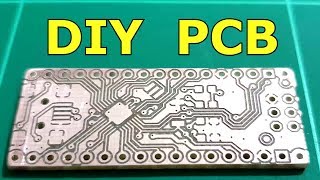
Make pcb with laser

Вставка
- Опубліковано 14 чер 2021
- Make pcb with laser engraver
Laser engraver is Laser cnc machine 50W, use 50% of 50W to engrave paint in copper layer.
-------------------------------------
Part to make:
1. PCB copper amzn.to/3rrFKLZ
2. Paint spray amzn.to/3poJ08r
3. Copper etchant amzn.to/3BH02p8
3. Laser cnc engraver amzn.to/3xgAiNG - Наука та технологія


It is curious how some people upload videos that are so confusing and apparently refuse to give the information totally. The paint you are using is Rust Oleum (the one I prefer), definitely NOT a single spray paint. This is a very special polyurethane paint that has a remarkable finishing for the price with lots of alternatives, colors and textures. Use black semi-brilliant finishing. Mate won't work the same. Should be applied 30 cm away from your target with a continuous horizontal sweeping movement. Don't apply more than one even thin layer, you are not painting a wall. You just want to evenly cover the copper side but after LASER burns the paint it doesn't remove it completely. This guy skipped showing a VERY IMPORTANT step which is cleaning the excess paint with a Scotchbrite like sponge (the hard side), very slowly and softly with water and dishes detergent. Caution not to remove the tracks...just the burnt paint. Copper should be exposed, if not the acid won't remove it. This step is the hardest, believe me. This paint dries in 30 minutes but needs some more time, about 1 or 2 hours to be LASERed. 24 hs wait gives the best results. Don't use any window paint. This guy has a misaligned machine, probably lose belts, as it shows awful straight lines. 5W LASERs work fine, focus is important, clean lens also, I use power 100% and slow speed 500 mm/s. This method works, it takes long times, depending of board size. A 20 x 10 cm board could take 3 hours with 600 dpi resolution and 12000 lines/mm. Don't use thin tracks. Less than 30 mils won't work. Best results 50 mils, round 100 mil pads, because the process tends to give thinner primitives. Surface mount SMD takes a lot of practice to get usable and solderable pads, unless you want to practically rebuild and retouch the whole PCB with a suitable PCB marker pen. There are lots of details and all are very machine and elements dependent.
too much arguments, I did the same since 3 years ago, I use enamel paint, no matter if is glossy or mate. the paint dries in a couple of minutes, The laser is 2W. I recommend that you make your own video and explain your success cases and worries. :) I will do the same on my future makings.
is it the best video out there with the best explanation?, no! but is it the worst video out there?, no! either way, it doesn't really matter what paint you use or how you apply it,, simple facts of co2 laser, as long as the copper is covered by the paint regardless if it is even or uneven coats, it makes no difference, the co2 at low or full power will never mark the copper and you only need the thinnest layer of paint for the etching process to work, hell, people been using sharpie pens to make a copper etching mask for decades and that hardly provides even coats.
I make some pcb in this way but:
first of all - diode laser make rectangular shape of light in focal point, this make unable to do tracks thiner than 20 mils. But CO2 laser have not this disadvantage, especialy if it is tube laser, so you can focus your power in smaller point with gaussian distribute power. It is realy important if you want thin tracks.
Second - i was use ordinary black spray, first from at row in my local shop.
After fire tracks i always wash pcb - with some sopa and teeth brush and this was ok.
You can also may use positiv20 if you have small power laser.
With 12000 lines/mm you add some unintended zeroes. 12 lines per micrometer mean you have laser with length of emmited light equal 1000/24 = 42 nm, with it is far away UV, it is sotf roentgen waves.
With focal point in size of 0.1mm enough is 20 lines per mm. Any more lines and better resolutions doesnt give you better results.
Solutuion is easy - buy and instal cylindrical lens for square shaped light from laser. But it cost a lot.
Thank you for the excellent explanation.
Are diode lasers (Sculpfun 5 watts) good for this job? What speed and power should be used? Thank you
@@laconeccionvideo is diode laser work to make pcb ?
Interesting. One small hint though - when you use spray paint, always start off of the thing you are painting and move onto it. The first few drops can sometimes blob.
I am definitely going to try this.
Un très très grand merci pour ce tuto qui m'a enfin permis de faire mes propres PCB de qualité quasi professionnelle . L'opération avec le laser est relativement longue mais pour un résultat exceptionnel . Encore merci 👍👍👍
What software do you use? I have a Enjoywood model A10 laser engraver, and been using lasergrbl and lightburn to burn the lacquer off the pcb. I spent a lot of time trying software that will generate a file that can be used with lasergrbl or lightburn, and in the end I had to generate a png file. I used KiCad 6.0 for to make the pcb layout and export the output to a Svg file which I convert to png in InkScape. Problem is, that I can’t get a high enough resolution to make fine traces less than 1.5mm wide and the standard size pads in kicad. I use 25% power. Thin traces and small pads are jagged and not useful.
The scraping step at the end is giving me anxiety aaaahhhhh the traces
plz use thinner to remove the paint, its just so much better
What speed did you use? Does it work equally with my machine that is 40W (Optical 5.5W)? Thanks
Thank you for video! How powerful should the laser be?
This video is very Amazing 👍👍 I appreciate your work. 👍👍 Kindly post a detail video. Also post Your laser CNC in details... 🙏
Wonderfull! Can i do this with an creality falcon 10w laser?
Cool technique!
I wonder what is minimal width of traces you can archive with this?
Maybe you can improve this further by using paint remover instead of metal sponge to remove protective paint layer after etching. That way you will not scrape very fine traces from the board.
depends on which lens you are using on your co2 laser, and how well your beam is focused. typically, a cheaper co2 laser will produce a dot size of 0.1
what did you use to layout the board first?
Hi. is ortur laser master 15w suitable for pcb works as advertised on gearbest and thank you very much
Saludos! Cuanto tiempo tardo el láser en esa pieza?
does it work if I soldered ICs? or this is just artistic make
please could you tell me how you generate the PCB image?.
interesting idea!
my method of creating pcbs is to let my 3d printer draw them with a permanent pen which is somewhat simeple to do but min line width is 0.5mm which might be a bit thick for future projects, so i hope i can try your technique. Can you tell us what software you use to get the g-code?
btw, you can probably use any permanent marker instead of spray paint. it's cheaper, easier to remove (with alcohol) and gives perfect results as well
Just need laser cutter/engraver software. It converts from an image like an SVG file into the needed instructions to etch it with your settings.
spray paint is cheaper than permanent marker, the paint can be removed with thinner or acetone.
Asphaltum Varnish? I’ve used this for boards before, albeit applied *by hand.*
Hm. Does it possible to use 3d printer for making template?
I've never had good results with sharpies, ink comes off in the acid bath before the board is fully etched.
How to preapre the file from easyEDA or any design software ? can you share the process ?
Don't use raster imaging thing! It costs a lot of time and less resolution (Only advantage from this raster technique is drill holes). Use isolation routing over flatcam, create gcode for rouing and then use laserGRBL to import and route only isolations. There are a lot of videos out there with laser diode ones! I use 3018 pro and a 30 watt (optically 7.5 watt) 450 nm. laser module.
Focus is very important to create the minimum spot. If you want to use smaller focus, give less power (if it's a powerful laser diode (optical power > 2W)) or use 405 nm. laser module or use some type of lens to collaminate the beam to a smaller (circuler) spot.
hello, can you give me the name of the black paint used??
aww, i could have saved $10 on toner transfer paper and $16 on buying an iron. All I need was a laser engraver 😁 I could never get the tonor to stick properly. gonna try this
The part that scared me the most is using the steel wool to clean off the excess paint. Would acetone (nail polish/ paint remover) do the job? I’d much rather have to handle a second round of solvent than deal with cracked or delaminated traces on a board I spent over a day preparing.
right, acetone can handle the paint. It is because i don't want to use so much chemical substance, so steel wool is ok in this example
Yeah, saw on this with pain))
Yes this is obvious that the viewer would not know he was doing. What is the spray etc..
Hi, Thank's very much for your video.
I cannot see the type of your paint product since i do not have any account on Amazon may be. Anyway it does not show me.
Is it a simple mat acrylic paint?
Sorry for my english.
Thank's in advance!
Kind regards. Jean-Yves.
amazing result. For the paint do you think a marker would work? I also think some acetone at the end can do a great easier job at removing the paint, painlessly!
I have tried with different types of marker, Mainly ones that are supposed to be waterproof. The stickness on copper is very varying depending the brand, and the critical moment comes when inserting the pcb in the etching bath. If using markers, test different brands before etching the final pcb. I actually do not find the marker style interresting for smd footprints, and hardly suitable for dip packages :
- stickness seems to decrease as the paths get thinner. After the etching process, some paths needs to be reconnected.
- the tip of the marker rapidely damage itself as it is ripped on metal. Needs To be changed every 3-4 pcb to keep a good trace quality
- needs a pretty "tuned" system to maintain the marker vertical when tracing, clearance in the maintaining system will allow small deviation of the tip on the board. Critical for thin / precise traces.
I think the laser method is cheaper after a certain amount of pcb, more precise and reliable than marker style
No marker will not paint uniformly
Nopeee the result is dull if you use paint marker
hello, where can I find such a printer, can you send me the link please?
Can I cut epoxy circuit boards with a diode laser?
Diode laser has very weak power to cut pcb
which paint?
Which laser do you use for PCB making? Diot uv fiber or co2
CO2
I'm confused why so many still use chemical etching with a laser engraver-cutter. I have seen people invert the PCB design, burn away the copper around the necessary traces, and even burn holes for inserting the parts. I get it, you will need a fume extractor for the copper that is being burned away, but it eliminates the need for the acid etching step and would be so much faster.
Because my laser is not power enough to burn copper
Es ta muy bacano lo del láser pero que pena que le siga con la esponja lo que hace es debilitar más las pistas
:D demasiada tecnología para matarla con la malla de acero.
You are right
you can use Tamarind to clean the copper without scratching!
thanks
it's cool work but it lacks the precision of a 2$ service from jlpcb
is there an advantage of doing this, except being a lot of fun, a learning experience and a cool experiment? I wonder what motivated you to do this rather than taking e.g. conductive paint/markers. I never tried this because of toxic chemicals involved...
@@userou-ig1ze I'd say the advantage would be testing out an idea in a matter of hours instead of weeks. Of course, that would be simple circuits. A lot of times you wanna test SMD components that it's not easy to test on a breadboard.
@@brunogoncalvesbasto Totally the main reason why I bought a 3018
Try getting a $2 board from JLC. By the time I add the various fee's and shipping, I am never less than around A$10 per board if I buy the minimum of 5. I can cut the cost to around A$7-8 by choosing the slow boat freight, but the delay makes it not worth it. I am back to etching myself, and awaiting delivery of my shiny new 3018.
The JLC boards are still great value for the next step of pre-production, but for a proof of concept one-off, it's hard to justify the JLC cost for fast delivery, or long wait for the lower delivery cost.
Can i do it with 5.5w laser and without Ferric chloride? Reply plz
Laser 5.5W can only engrave paint, not copper on PCB. If you got 5.5W laser cnc, you can make PCB, but have to use FeCl3
@@engineer2you ok thanks
If you pre-make a hole for positioning.
Then you can not remove all the paint after etching.
After all, you only need contacts that can also be burned with a laser.
Hello from Russia.
Autant graver directement avec une fraise de 0.1mm c'est ne pas utiliser de produits chimiques
What brand is the spray?
it is general spray paint (for door, windows, etc...)
@@engineer2you no brand or anything?
@@timcheng144 any brand is OK
How is this useful if you don't explain what you are doing and why?
What is the purpose of the black paint ?
It protects the copper for chem-etching it after burning away the paint where he wants the acid to dissolve the copper. I don't understand why people are bothering to chemical etch boards when they can just use the laser to burn away the copper, and leave it intact where they want the traces. You'll need a good quality fume extractor since the burned copper will be toxic, but it sure as hell beats going through all this then still etching the board with acid afterward.
@@JonDeth - We use the resist and acid because we don't know it's possible to burn away the copper. That is not obvious, I have yet to find a video demonstrating this approach.
@@JonDeth - Okay, I found videos where they burn away the copper, but unsolved is what to do with the burned board that shorts all the traces together because of the conductivity of carbon?
@@jrstf carbon is an insulator, not a conductor. Modified carbon can produce conductors and semiconductor. No one is laser etching PCB's with the knowledge and ability to do so only to end up with a shorted out board kid! lol
*Typically, anyone worth their salt is designing their own PCB's from the ground up, and the circuit traces will have greater separation for a variety of reasons.*
My long term goal is primarily audio and radio equipment, so spacing out traces more than industrial and commercial production is a way to prevent potential noise from crosstalk between devices. *They jam all that shit together to save money and shrink equipment down in size.* If mfr. in the USA weren't lazy, greedy and somewhat retarded, they would be printing CPU's, microcontrollers and other devices because though larger in end product size, that increase in size also provides tremendous performance advantages.
Name of paint
General paint is ok
Where to buy this kind of machine?
It is laser cnc machine 50W, but 10W is enough
@@engineer2you el laser d emi cnc es de 5500 wattios como Haria??
I find a 40W CO2 laser at my local Maker Space. Always good to share.
What is the brown acid liquid?
Ferric chloride
This process is time waste and it's harmful for health, lazer engraving can do the complete process no need to use etching
Agreed. Use the laser to burn away unneeded copper, leave copper where it will be the circuit traces, and run a fume extractor to remove the toxic burned copper. They do all this work then still use acid to dissolve the copper and must dispose of this toxic sludge afterward.
@@JonDeth okay
Don't you know about sandpaper?
I honestly dont see a purpose. If I actually have to etch it, I will do stripped photo-litographic process with photoresist like most of the guys at home do. If I use CNC, I would like to have ready-for-coating microstrips after, not etching + removing the mask like I do regularly.
Hi engineer, you cheated a little. Where are the paint residues that are clearly seen at 1:20?
Use laser engrave 2-3 time. Paint will be clear
Miracle... 1:13 I see a different image from 2:23. Maybe I'm wrong ??? :)
I saw same that you saw. Very strange, confused me.
Options:
a) wait two weeks for JLC
b) do this sort of shit, which though undeniably cool is not where I want my engineering effort to go
c) move to Shenzhen...
This video is pointless. What paint are you using ? What laser settings are you using ?
See video description please