
Вставка
- Опубліковано 28 чер 2024
- In this episode Shahriar takes a close look at a wireless-Ethernet product based on Qualcomm's 60GHz WiGig chipset. The episode is inspired by the upcoming in-person RFIC & IMS IEEE conferences held starting June 19th, 2022 in Denver, Colorado, USA:
IEEE Radio Frequency Integrated Circuits Symposium:
rfic-ieee.org/
IEEE International Microwave Symposium:
ims-ieee.org/ims2022
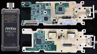
The entire WiGig system architecture is analyzed end-to-end. The phased array module is presented using x-ray images and individual RFIC's are examined under microscope.
www.TheSignalPath.com
/ thesignalpath
www.Patreon.com/TheSignalPath - Наука та технологія


PLEASE do more videos like this. Zooming way in and pointing out the semiconductor features was incredibly helpful for me as someone who knows the circuit design but never works with IC layout.
I think he's mentioned a few times that it gets a bit too close to the IP at his day job. But yeah, I'd love to see more
TSP: Comparatively LOW frequency - Only 15GHz
Me: Comparatively HIGH frequency - Almost 40MHz
Masterclass! Please do more Videos like this, even if the audience is smaller. Maybe Take another look at the Starlink Asics ;-)
I second the starlink rfics
Yes that would be interesting. Also the starlink chips use digital beam forming.
Thank you for making this video. Next time can you please put together a basic block diagram to help those of us who haven't designed phased arrays follow along? It would be very helpful to see what part of the block diagram you are tracing through the layout.
I had to deal with phased array antennas in a very different context. Regional deep hyperthermia. It uses three rings of four antennas to deliver energy into the human body noninvasive. My job was the treatment planning software which also included an EM-Simulation. I am a software developer so I contacted HF specialists to support me in writing a MAXWELL solver. Was really interesting... too bad the company foundout after eight years that there is really no target market for a niche product such as regional deep hyperthermia. Back to your topic. All this black magic about Network analysis and how antennas start talking to each other and the complications setting up high frequency antennas are interesting as long as I am far enough away from the battlefield. These devices operate at 100MHz... but 60GHz??? Thx for the nice video!
i participated in a similar project in uni but at 433 mhz
Your collection is incredible!
Congrats on 100K subs. It has taken a while but very well deserved.
Wow, stunned by the detail there in. Thanks so much for the really great explanation and the outstanding xray and microscope images you capture.
You mentioned that the design and tape out is all done by hand. Ok. Mind officially blown! See you at IMS.
I appreciate your work and I love your videos. Congrats on 100k! I am following for a long time, you should have gotten to 1M by now in my opinion. I guess there are fewer people seeking knowledge than entertainment here. Nevertheless, keep up the good work, there are a lot of people who enjoy your work :)
Very cool. I always love seeing RF and mixed signal dies. I would be curious about how these mixed signal ICs are actually designed-- is it done semi-manually similar to a PCB (eg. with a symbol library but a human still has to place and route each block), or does it use some kind of HDL like Verilog? My understanding was that most digital ICs/ASICs could be designed almost entirely in HDL, maybe with some manual tweaking after whatever program synthesizes the design, so curious how it's done for analog and RF ICs.
What is the make and model of the microscope you are using? Those images are superb!
Carl-Zeiss Axioskop with Differential Interference Contrast Microscopy capability. He did a video on it. TNP #3.
They look to be about $7,000-$10,000 used on ebay. I'm sure they're a bit more than that for a new one.
Thanks for the walk through! You managed to make a pretty map actually seem like something to this non-EE. 👍️
Very intriguing and beautiful design, thanks for the video!
Amazing stuff. Thanks for sharing the insights in these complex technologies.
Wow, what a masterclass!
Thanks!
Great video, and impressive in how can you go through so much elements, talking very fast and yet be very clear.
I'm just amazed there are people like you that can look at those minute structures and "read" them like if they were looking at an schematic diagram.
I understand the rational as it's much the same way as we do when we look at a PCB and reverse engineer it mentally while troubleshooting a circuit, but on the chip, the difference between the actual "components" and the interconnects are so much subtle.
It's really impressive.
Big Awes to that!
Perfect! It's so useful. Please make more videos.
Very interesting! Please make more in-depth videos like this.
Awesome video!
Never mind the RF, this microscope is amazing!
Even reading comments are very informative.
Thanks for the video.
I'm captivated by this video
Really Great Stuff !!
Having struggled through my undergraduate antennas course this past semester, I'm laughing that this video decides to be posted as the semester ends. Im trying my hardest to follow along.
Congrats on 100k subs!
Hi Ashmi! :)
This is one of the best electronics channel I follow. Congrats for your hard work and for making easier to understand such complex topics for "slow-mo" guys like me. BTW I hope this is not restricted because of TELCO p0*n Content...
Fascinating, but way over my head.
awesome video.
Contrast on the XRAY looks so good.
Can guess that the 2 VCO's and duplicated arrays are to get 16 channels out, but they only pulled out 8 from the chip to the board, switching the other side off in firmware, and also only using 3 of the ones on the board. Likely there is a version of the control board that can drive 2 arrays at the same time, so having the 2 separate modules allows then to be interleaved, to get 2 totally separate beams out at the same time, allowing a single unit with patch antennas all round at 15 degree intervals, to act as a repeater for the system, allowing relay from one to the other down the route easily.
nice! somewhere in the near future!
Wow, awesome video. I could watch you for hours explaining the IC. What I found a bit strange was the fact that some of the antennas were connected on the left side and some on the right side. This will probably flip the field bei 180°, you can for sure compensate that in the software, but I cannot see any reason why they did that.
impressive
First, congratulations on the 100k subs.
Second, this was a piece of art.
The amount of knowledge in this video is really embarrassing. With this video like these you're really educating people about black magic and show them that it's not that black it's fairly simple. Btw that's a beautiful collection of test equipment.
Thank you Shahrihar !
One small request, would plz put the links for the publications, diagrams, and datasheets you show in your next videos in the video description ?
Thank you again.
I would love a video explaining how to spot integrated structures
WoW,, I hope one day I can work in designing circuits at The silicon level I would love to work in a lower abstraction layer to really gain the knowledge .
WOW Santa 🎅 Bring you Tons of Test Equipment, your lab is huge as mine 😉 of old Test Equipment but its the good old days 1960s 1970s 1980s & 1990s,
I worked on RADAR that's really when I learned a lot of amazing RF - Microwave magic 😉👍
ASIC metal layers look so beautiful and complex. Are those big tracks with dog-bone shapes are just ground to shield sections, just like metal shields and boxes on RF PCBs?
Incredibly informative video
I would really like to see a video on the different methods of digital phase shifting
it has always fascinated me but i cant find good resources on the methods
That antenna chip had to have take quite some time to design, holy shit the amount of coils and stuff in it. They have a lot of help by the program used for it but it sure take time anyway.
What microscope are you using? The interference microscopy is super cool!
Carl-Zeiss Axioskop with Differential Interference Contrast Microscopy 😉
Very nice, I like the reverse engineering of the system.
It would be very intersting to get more videos of this style maybe also of some "conventional" wifi routers, cellular basestations, etc.
I also really liked your video on cellular power amplifiers from a few years back.
Thanks for all the effort, that went into this video.
I think under 5 GHz is pretty much DC for him, so I wouldn't expect much content in that range... :D
@@szaszafaja
Judging by the the statement he made "15GHz is a very low frequency, relatively speaking" you might be pretty much spot on ;)
This video inspired me to give up on my semi conductor design ambitions :)
I have many questions about dc dc converters on the ship ...
Did you discussed this before ??
Or how can I learn more about that topic ?😃
you have a lot of waveguide technology here, it would be nice to have a reminder about it for your viewers. all these runs and trafic lines would make more sense,, great video
وجود امثال شما برای اینده ایران و قتی که حکومت اخوندی سرنگون بشه یه نعمت بزرگ است
Wow! This was awesome! Please do more deep dive reverse engineering videos on silicon level!
Shahriar thank you for the in-depth look at the Qualcomm,s Ethernet transceiver would it be located in a business environment. Or is it a typical repeater-type setup between Nodes? Microwave tech for me is in the dark arts category. It is incredible what goes into a chip to achieve the desired outcome.
It is a simple wireless ethernet product. They also make them in dish format.
One part that remains untouched is how the phase is made ? How is beam steering done on this device?
I just got permission to go to IMS from my manager! Hope to see you there
Million dollar backdrop 🥰
Great video
Can i get a reference to that paper you showed ?
Shout out to Latvian company mikrotik for some great products! Namely the RouterBoard and RouterOS
Amazing reverse engineering of the chips! I wonder if the large inductor at 21:21 could be a quarter wave stub at 15GHz to suppress IF leakage, or even 7.5GHz to spread the reference?
Anyone remember quantenna? I hated their radio, took minutes to boot while my router waited for it
1:50 You're saying it like that - "it supports power over Ethernet". But Mikrotik devices are notorious for their shitty PoE-support. For example, the LoraWAN node I run at the office is a RBwAPR-2nD. That only supports a questionable passive PoE-variant, where I use an active PoE extractor to get 12V, and then feed it back into the Ethernet port with a passive PoE-injector. Otherwise the device will not work. What's even worse, it might get damaged if you supply proper 48V PoE.
What microscope are you using?
I was using the HMC6300 chip set a few years ago, and IIRC the 60 GHz band is broken into 13 channels. Maybe the dual LO is to hop quickly between channels.
Hi Louis, I will make a short video about the upgraded microscope.
WOW
Being an audio frequency analog electronicsa gal, I marvel at microwave engineering - the impressive complexity and somewhat elegant simplicity of VHF PCB design. You know your thing, I don't, and I've got to take ytour word on that one.
Omg. @Keri Szafir Marry me. We will make sweep LPF and OpAmp babies through our uSmas and can go fetng all day 🥰
@@derrekvanee4567 nah, I mostly do vacuum tube amps and old radios :)
which ic they used for powering the cpu? thanks
Would it be possible for you design a simple RF based IC for a video. Just in software no actual hardware. Would be really interesting for me. Im currently studying EE and would like to know how the process looks like. Or will there be problem surrounding software licensing etc.?
I think sending DC seperately might make multiplexing a bit easier
There is some place for more shelving just under the ceiling, you know.
Yes! We must stack higher!
I saw dude (Evil monkey design) using soldering rosin for dissolving packages.
Where is your oil paint of the Enterprise NCC-1701-D ? 😮
It is still on the wall. This video was shot at a different angle. :)
Inastead of using nitric acid for dissolving the IC plastics package you can use hot dimethylformamide. Its poisonous too but not such a mess as the acid.
I will certainly try. Thanks!
@@Thesignalpath Don't expect the plastics dissolves smoothly. At first, there appear cracks in the surface, then the plastics (mostly epoxy) starts crumbling. By carfully removing the bits and chips with a needle or similar you slowly working forward to deeper regions. after quite some time you end up cleaning the central parts. Be careful not to scratch the silicon. Good luck!
At 30:00 where you are showing the amplifiers/switches, are those huge network of parallel MOSFETs that are doing the amplification? Im struggling to understand what the topology of those amplifiers is
At mm-wave amplifier topologies tend to be fairly simple. These are all likely common-source amplifiers.
@@Thesignalpath thank you!
i once made an fm transmitter with a transistor
it did not work
This damn man has $10M of measurement gear behind him.
He buys broken equipment on ebay, and then he fixes the them!
@@rharriszzz Plus he uses $50 million at his job, though likely his home equipment is just a subset of what he considers to be the "basic minimum" needed to work from home....
If someone does - he fully deserves it!
Would Xylylene have dissolved the potting material.
👍👍
Hey Shahriar, right around 34:00 I couldn't hear what you said. You are looking at an inductor and note that it needs very high quality factor. What is it for?
Says VCO, then he says "culprit"??
It is the core of a Colpitts VCO.
@@JohnMullee I think I figured it out, a "Colpitts oscillator" is a part of a VCO that does indeed require a high Q factor inductor
en.wikipedia.org/wiki/Colpitts_oscillator
Do you photograph the chip and look at the stored image or you observe it live. @28:20 if not live how r you able to change focus
It is all live.
@@Thesignalpath nice, but the chip holders were not visible at all. I would like to see an episode on ur microscope/optics.
@@lolvivo8783 What are chip holders?
@@Thesignalpath i mean u have to mount the module in the xray box @ 13:15 to navigate and orient. That apparatus would have to clamp/hold the module in place; that is what i meant by chip holder.
I see no such clips or holding apparatus @ 13:45 or any other images.
good evening, tell me what the article is called and can I download it?
In what CAD would such a chip be designed? ADS? I suppose vanilla Cadence doesn't have support for all this funky RF stuff.
Several CAD tools are involved. Final layout is in Cadence. But EM many other tools along the way are used for simulation, EM modelling, extraction, etc.
May I ask why the IC under the microscope is made up of many colors i.e pink, green, purple etc.
We have internal reflections and diffraction from the IC because of the changes in dielectric constants & the fact that the dimensions/layer-to-layer distances are comparable to visible light.
👍🙏
looks like super mario 3 world maps
When using acronyms, could you be sure at least once each video to clarify what the acronym stands for? Thanks!
Sure.
Amazing you can buy this for around 200 usd!
Mmmmm denver is a bit far for me. But i like the idea of a conference. Does anyone here know anything similar in western europe( the netherlands)?
European Microwave Conference!
Duh, I am so embarrassed not being able to invent and manufacture such components on my own!
If I am not mistaken, Mikrotik is not owned by Qualcomm. I have worked with similar modules and believe this is NOT a steerable phased array, but fixed staring based on our network tests. Is the antenna not LTCC substrate? The design I worked with had a 5.8 Radio as the IF and it appeared that the 60 GHz end was a block up/down converter. The BW was about 18 degrees. The EIRP from the substrate was about 10 dBm. It did sweep in frequency for acquisition. I am not sure the paper that you used for the reference design applies to this module.
It is steerable. The EIRP per array is over 25dBm including antenna gain.
It is definitely steerable and the publication is the correct reference for this chipset. The part number of the IC can be seen on the die.
27:00 This looks more like vias than anything else. You can see at the bottom of the image there's power and ground busing on the next metal layer down, lining up with the grids of vias.
CMP filler is relatively rare on the topmost metal layer as most processes do not planarize the wafer after patterning it. Why would you? There's no more lithography to do other than glass cuts for bond pads, which are very low resolution so there's no concern about limited depth of field. The topmost metal layer is normally aluminum rather than copper, so you can pattern it with a dry etch rather than needing a complex damascene process.
27:15 The slits here are not for manufacturing reasons either. These actually improve the longevity of the device by increasing resistance to electromigration. Mass transport in electromigration is predominantly parallel to grain boundaries in the metal; if your average wire width is less than the grain size then grain boundaries are mostly perpendicular to your current flow and thus you get less metal being carried along with the current.
The dark "hole" looking things on the top metal layer are vias. The other wholes are for density.
The slits are also for density & stress. We do this regularly for wide metals. The DRC tool flags both density & stress requirements. You cannot fabricate unless you meet these rules. The slits are not for electromigration. Electromigration is a function of current density and exponential function of temperature. We spend a lot of time trying to meet electromigration rules. If you have any reference for what you are saying, I'd like to see it.
@@Thesignalpath Interesting! Doing a bit more reading it seems we're both half right re the slits - their primary purpose is indeed stress relief, but they also promote formation of bamboo grain structures which has a beneficial side effect WRT electromigration.
One can always make the lowest band of a multiplexer dc-coupled (e.g. with a low-pass filter), so there should be no need for a quadruplexer to split/combine the "Control Signal" band with dc, i.e. a triplexer would suffice. My guess is that the dc-handling of the filtering components was not sufficient to pass the required dc currents and that is why they chose a separate dc line.
Well finally two likes in one day, hahahahaha
That device can up to 8 SMs connected with a 180 degree phased array
It was designed in Israel. Whoever designed that can afford a house.
Correct Wilocity design. en.wikipedia.org/wiki/Wilocity