How to Spin Photoresist onto Wafers and Pieces

Вставка
- Опубліковано 25 гру 2019
- In this video you'll learn the preferred KNI way to spin photoresist onto wafers and pieces using the KNI's Laurell brand spinners. You can learn more about using resists and lithography in the KNI on our Lab wiki, by visiting the Optical Lithography Resources page (bit.ly/2PUnkjW) and touring the Lithography Equipment (bit.ly/377Xf6U). Also see the KNI's Spinner Rules (bit.ly/2SpEAPU), a written SOP on how to clean the spinners (bit.ly/2QufwEP), and the Laurell Manuals (Lite Version: bit.ly/2QlkbZm & Long Version: bit.ly/2PVTFXD).
The video includes how to:
1. Select and verify a spin recipe (0:56)
2. Inspect and clean the spinner (1:40)
3. Spin-clean the wafer and pre-bake (2:37)
4. Prepare wafer surface with HMDS, if necessary (3:55)
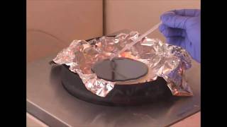
5. Load wafer onto chuck, apply resist, and spin (4:55)
6. Remove resist edge bead (6:30)
7. Post-bake the wafer (7:22)
8. Clean the spinner (7:38)
9. Exchange in/out various vacuum chucks and adapters(9:23)
10. Spin resist onto a small piece (10:30)
11. Document the parameters of your run in the log book (13:07)
12. Replace a vacuum chuck or adapter o-ring, if necessary (13:50)
___
Disclaimer: This video is intended to serve as supplemental information and cannot replace in-person instrument training. Caltech and KNI are not responsible for how the presented information is translated for use in other facilities.
For information or questions about this video, contact kni@caltech.edu - Наука та технологія


Bravo for this
what is the material of the pipette to dipense the photoresist? Does it need to be high density polyethylene (HDPE)?
Thikness of film seems to be not uniform 7:12.. What reasons could lead to that?
Comet mark on the edge is caused by particle contamination. Chuck mark on center of the wafer is caused by difference in temperature due to evaporative cooling (chuck provides better thermal conductivity to chuck/wafer/photoresist stack, so center of the wafer is warmer than edges).